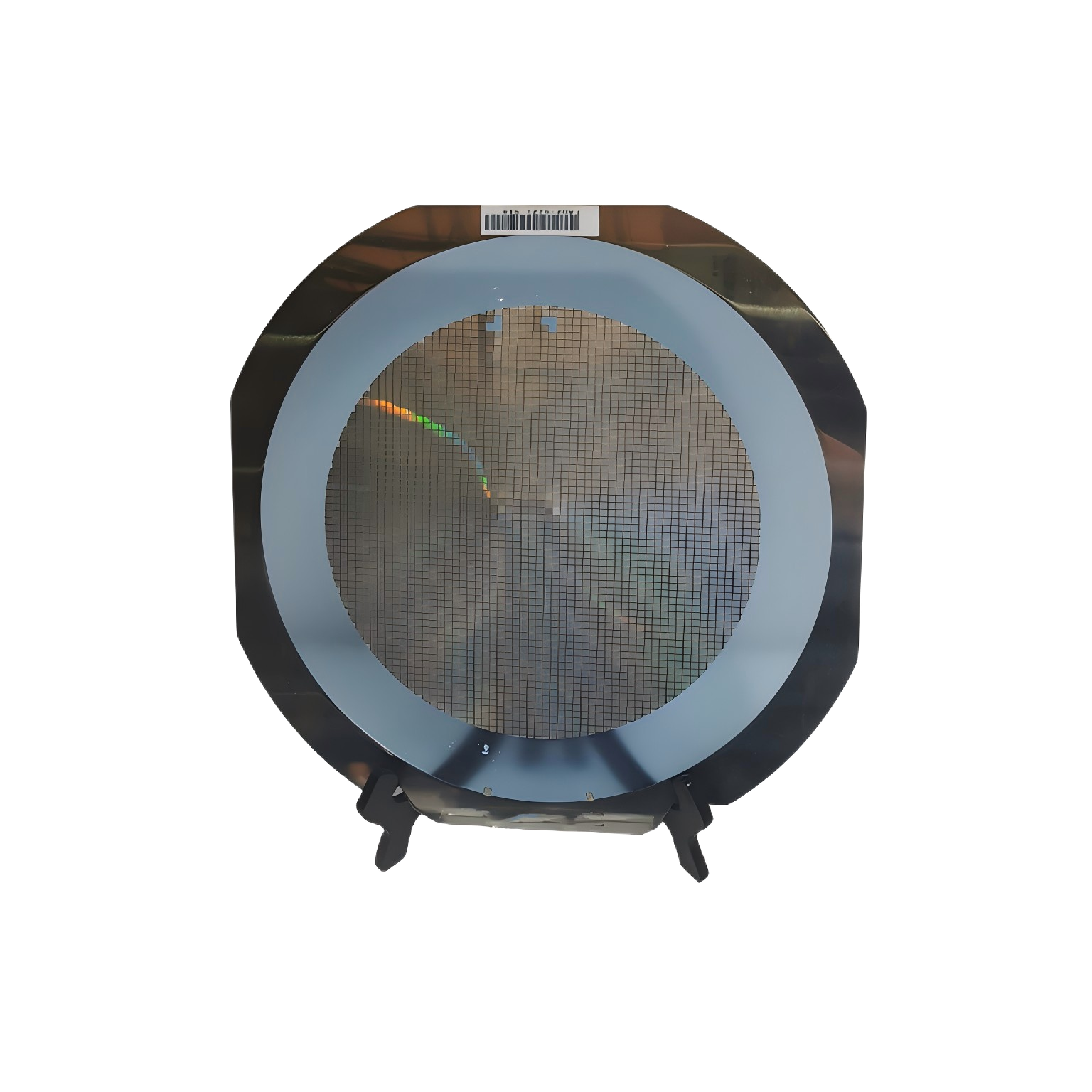
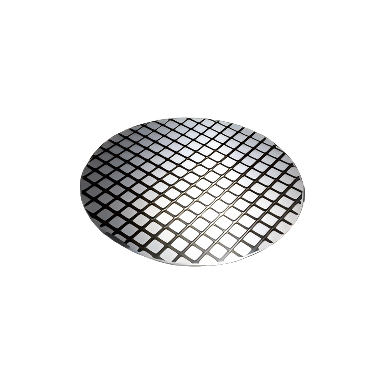
6 Inch Wafer Solutions: Advanced Semiconductor Manufacturing Platform for High-Performance Electronics

All Categories
Get a Quote

Get a Free Quote

Our representative will contact you soon.
Email
Name
Company Name
Message
0/1000

6 inch wafer

The 6 inch wafer represents a fundamental component in semiconductor manufacturing, serving as the substrate foundation for creating integrated circuits and electronic devices. This circular silicon disc, measuring precisely 150 millimeters in diameter, functions as the base material where millions of transistors and electronic components are fabricated through sophisticated photolithography and etching processes. The 6 inch wafer has established itself as a critical element in the production of various semiconductor products, including microprocessors, memory chips, sensors, and power management devices. Its standardized dimensions ensure compatibility across different manufacturing equipment and facilities worldwide. The technological features of the 6 inch wafer include exceptional surface flatness, uniform crystal structure, and minimal defect density, which are essential for achieving high-yield production rates. These wafers undergo rigorous quality control processes to maintain consistent electrical properties and structural integrity throughout the manufacturing cycle. The crystalline silicon structure provides optimal electrical characteristics, enabling precise control over dopant distribution and junction formation. Modern 6 inch wafers incorporate advanced purification techniques that reduce impurities to parts-per-billion levels, ensuring superior device performance and reliability. The manufacturing process involves growing single-crystal silicon ingots using the Czochralski method, followed by precise slicing, polishing, and cleaning procedures. Applications for the 6 inch wafer span numerous industries, from consumer electronics and automotive systems to industrial automation and telecommunications equipment. The wafer serves as the platform for creating complex integrated circuits that power smartphones, computers, medical devices, and IoT applications. Its versatility makes it suitable for both analog and digital circuit fabrication, supporting diverse product requirements across multiple market segments.

Popular Products

The 6 inch wafer offers significant cost advantages compared to larger wafer formats, making it an ideal choice for companies seeking efficient semiconductor manufacturing solutions without excessive capital investment. Manufacturing facilities can operate 6 inch wafer production lines with lower equipment costs and reduced facility requirements, translating to substantial savings in operational expenses. The smaller format allows manufacturers to optimize production volumes for specialized applications and niche markets where flexibility matters more than maximum throughput. Production yields remain consistently high with 6 inch wafers due to their manageable size, which reduces the probability of defects affecting entire wafer surfaces. This reliability factor ensures predictable manufacturing outcomes and minimizes waste, contributing to improved profitability for semiconductor companies. The 6 inch wafer format provides excellent scalability options, allowing manufacturers to adjust production capacity based on market demand without committing to large-scale infrastructure investments. Processing times are optimized for 6 inch wafers, enabling faster turnaround cycles and improved responsiveness to customer requirements. The established ecosystem surrounding 6 inch wafer technology includes mature equipment availability, proven process recipes, and extensive supplier networks, reducing implementation risks for new manufacturing initiatives. Quality control becomes more manageable with 6 inch wafers, as inspection and testing procedures can achieve higher precision across the smaller surface area. The format supports diverse product portfolios, from high-volume consumer electronics to specialized industrial applications, providing manufacturers with strategic flexibility. Energy consumption per processed wafer remains lower compared to larger formats, contributing to sustainable manufacturing practices and reduced operational costs. The 6 inch wafer standard has proven its reliability across decades of semiconductor evolution, offering manufacturers confidence in long-term technology roadmaps. Supply chain stability for 6 inch wafer materials and equipment ensures consistent availability and competitive pricing structures. Manufacturing expertise for 6 inch wafer processing is widely available, reducing training requirements and enabling faster production ramp-ups for new facilities.

Latest News

Achieving Peak Performance: How High-Speed ADCs and Precision Amplifiers Work Together

07

Jan

Achieving Peak Performance: How High-Speed ADCs and Precision Amplifiers Work Together

In today's rapidly evolving electronics landscape, the demand for precise and rapid signal processing continues to grow exponentially. From telecommunications infrastructure to advanced measurement systems, engineers are constantly seeking solutions ...
View More
Building Reliable Systems: The Role of Precision Voltage References and LDOs in Industrial Applications

07

Jan

Building Reliable Systems: The Role of Precision Voltage References and LDOs in Industrial Applications

Industrial automation and control systems demand unwavering accuracy and reliability to ensure optimal performance across diverse operating conditions. At the heart of these sophisticated systems lie critical components that provide stable power mana...
View More
Domestic High-Precision Linear Regulators and Instrumentation Amplifiers: Low-Power Design for Replacing Imported Chips

02

Feb

Domestic High-Precision Linear Regulators and Instrumentation Amplifiers: Low-Power Design for Replacing Imported Chips

The semiconductor industry has witnessed a significant shift toward domestically manufactured components, particularly in the realm of precision analog circuits. Domestic high-precision linear regulators have emerged as crucial components for enginee...
View More
Super-junction MOSFET

25

Jan

Super-junction MOSFET

The super-junction MOSFET (Meta Oxide Semiconductor Field Effect Transistor) introduces a lateral electric field control on the basis of the traditional VDMOS, thereby making the vertical electric field distribution approach an ideal rectangle. This ...
View More

Get a Free Quote

Our representative will contact you soon.
Email
Name
Company Name
Message
0/1000

6 inch wafer

Superior Manufacturing Efficiency and Cost Optimization

Superior Manufacturing Efficiency and Cost Optimization

The 6 inch wafer delivers exceptional manufacturing efficiency through its optimized size that balances production capacity with operational flexibility. Manufacturing facilities benefit from reduced equipment footprint requirements, allowing companies to establish production capabilities without massive capital expenditures associated with larger wafer formats. The processing efficiency of 6 inch wafers stems from their manageable dimensions, which enable precise control over manufacturing parameters and consistent process outcomes across entire production batches. Equipment utilization rates improve significantly because processing cycles complete faster, allowing higher throughput of finished products within shorter timeframes. The 6 inch wafer format reduces material waste through improved yield rates, as defects typically affect smaller portions of the wafer surface compared to larger alternatives. Cost optimization extends beyond initial equipment investment to include ongoing operational expenses such as utilities, maintenance, and consumables. The established manufacturing infrastructure for 6 inch wafers provides access to proven process technologies and equipment configurations that minimize development risks and accelerate time-to-market for new products. Facility requirements remain modest compared to larger wafer fabs, enabling companies to locate production closer to target markets and reduce logistics costs. The mature ecosystem surrounding 6 inch wafer technology includes comprehensive supplier networks, standardized equipment interfaces, and extensive process knowledge databases that streamline manufacturing operations. Quality assurance processes become more efficient with 6 inch wafers due to faster inspection cycles and improved defect detection capabilities across the smaller surface area. Energy consumption per unit of processed silicon remains lower than larger formats, contributing to sustainable manufacturing practices and reduced environmental impact while maintaining competitive production costs.
Exceptional Versatility for Diverse Applications

Exceptional Versatility for Diverse Applications

The 6 inch wafer demonstrates remarkable versatility across multiple semiconductor applications, supporting everything from high-performance computing chips to specialized sensor devices and power management solutions. This adaptability makes the 6 inch wafer an ideal platform for companies developing diverse product portfolios or serving multiple market segments simultaneously. The wafer format accommodates various circuit designs, from complex system-on-chip architectures to simple analog circuits, providing manufacturers with strategic flexibility to respond to changing market demands. Different semiconductor technologies integrate seamlessly on 6 inch wafers, including CMOS, BiCMOS, and specialized process variants for RF, power, and sensor applications. The standardized format enables efficient production planning and inventory management across different product lines, reducing complexity and operational overhead. Research and development activities benefit from the 6 inch wafer platform through cost-effective prototyping and small-volume production capabilities that support innovation cycles. The format supports both mature and emerging technologies, allowing manufacturers to leverage existing production infrastructure while developing next-generation products. Customization options remain extensive with 6 inch wafers, enabling tailored solutions for specific customer requirements without compromising manufacturing efficiency. The wafer size provides optimal die yield for many common chip sizes, maximizing the number of functional devices per wafer while maintaining acceptable defect rates. Mixed-signal applications perform exceptionally well on 6 inch wafers, as the format provides sufficient space for complex analog and digital circuit integration while maintaining signal integrity. The platform supports various packaging options and assembly techniques, from traditional wire bonding to advanced flip-chip and wafer-level packaging solutions. Testing and validation procedures are streamlined with 6 inch wafers, enabling faster qualification cycles and reduced development costs for new product introductions.
Proven Reliability and Market Maturity

Proven Reliability and Market Maturity

The 6 inch wafer technology has established an unparalleled track record of reliability through decades of successful deployment across the global semiconductor industry, providing manufacturers and customers with confidence in long-term technology investments. Market maturity brings significant advantages in terms of supply chain stability, with multiple qualified suppliers offering consistent material quality and competitive pricing structures. The extensive knowledge base surrounding 6 inch wafer processing includes comprehensive process libraries, failure analysis databases, and best practices documentation that accelerate new product development and reduce technical risks. Quality standards for 6 inch wafers have evolved to extremely high levels, with defect densities and material specifications that meet the most demanding application requirements. The mature manufacturing ecosystem ensures access to qualified equipment, consumables, and support services from established suppliers with proven performance histories. Risk mitigation becomes more manageable with 6 inch wafer technology due to the extensive operational experience and documented reliability data available across the industry. The format has successfully adapted to evolving semiconductor requirements while maintaining backward compatibility with existing production infrastructure and processes. Regulatory compliance and qualification procedures for 6 inch wafer products are well-established, simplifying certification processes for applications in automotive, medical, aerospace, and other regulated industries. The technology roadmap for 6 inch wafers continues to evolve with industry requirements, ensuring continued viability for future product generations and technology nodes. Supply chain resilience benefits from geographic diversity of 6 inch wafer suppliers and manufacturing capacity, reducing dependency risks and ensuring consistent material availability. The mature market provides extensive benchmarking data and performance metrics that enable accurate production planning and cost modeling for new projects. Technical support networks for 6 inch wafer processing are comprehensive, with experienced engineers and application specialists readily available to assist with process optimization and troubleshooting activities across global manufacturing locations.

Get a Free Quote

Our representative will contact you soon.
Email
Name
Company Name
Message
0/1000