High-Performance MOSFET Wafer Solutions - Advanced Semiconductor Technology

All Categories
Get a Quote

Get a Free Quote

Our representative will contact you soon.
Email
Name
Company Name
Message
0/1000

mosfet wafer

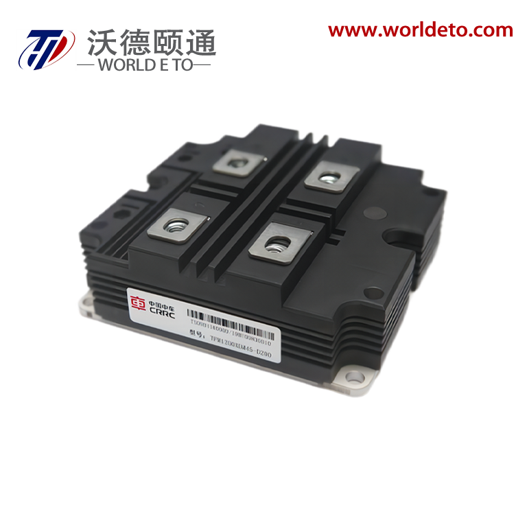
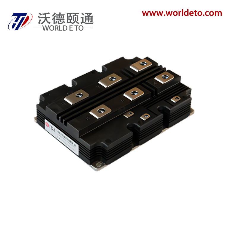
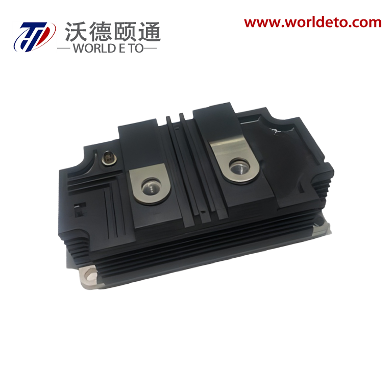
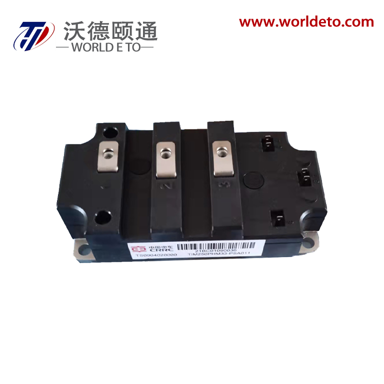
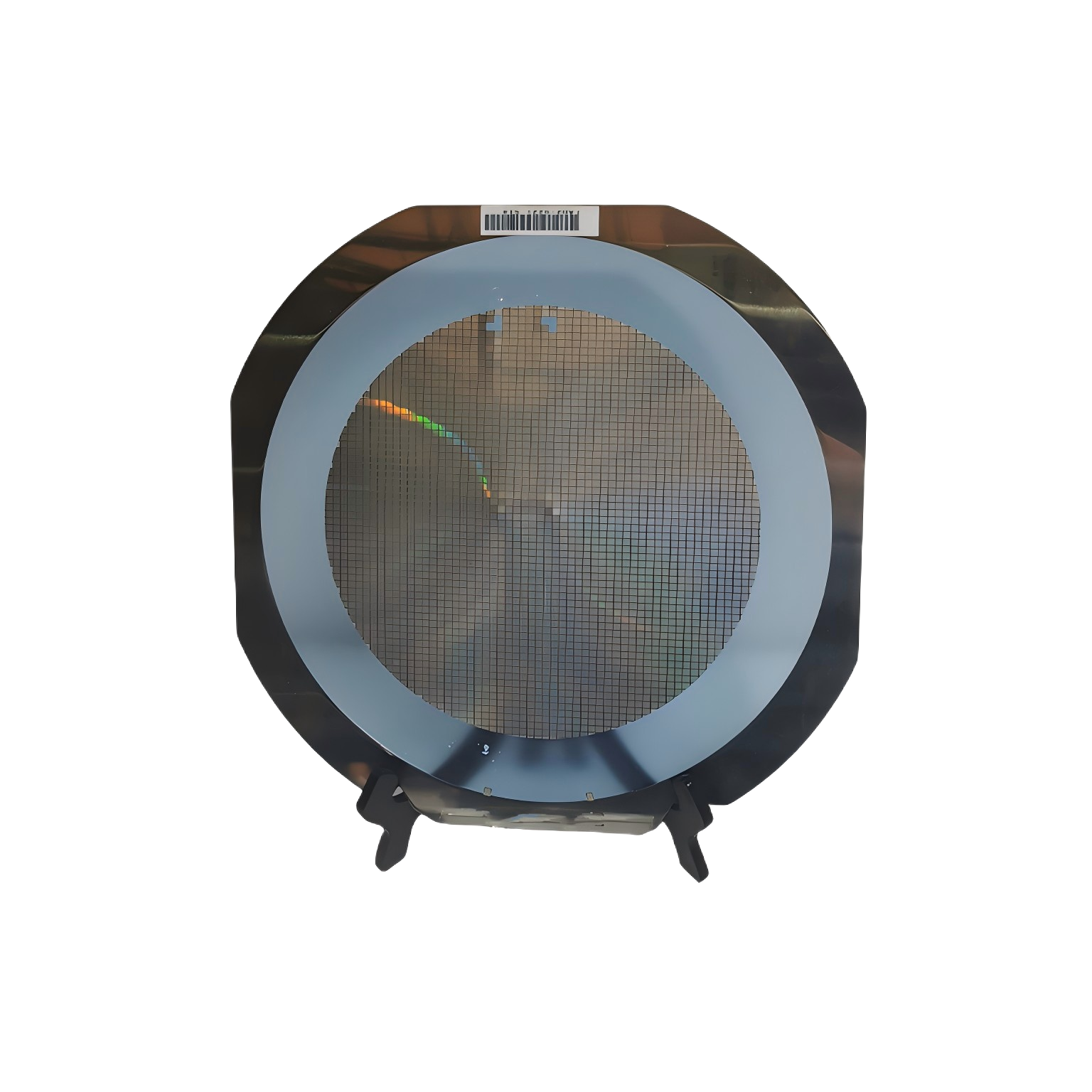
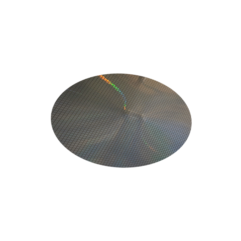
The mosfet wafer represents a fundamental building block in modern semiconductor manufacturing, serving as the foundation for creating Metal-Oxide-Semiconductor Field-Effect Transistors. These silicon-based substrates undergo precise fabrication processes to produce millions of individual MOSFET devices on a single wafer surface. The mosfet wafer begins as ultra-pure silicon crystal, carefully grown and sliced into thin circular discs that provide the perfect platform for semiconductor device construction. During manufacturing, multiple layers of materials are deposited, etched, and doped to create the complex three-dimensional structures that define MOSFET functionality. The primary function of a mosfet wafer centers on voltage-controlled switching and amplification capabilities. Each transistor formed on the wafer consists of source, drain, and gate terminals, with the gate electrode controlling current flow between source and drain through electric field manipulation. This fundamental switching mechanism enables digital logic operations, power management, and signal processing applications across countless electronic devices. Technological features of the mosfet wafer include exceptional miniaturization capabilities, with current manufacturing processes achieving transistor dimensions below 10 nanometers. Advanced lithography techniques allow precise pattern definition, while chemical vapor deposition and ion implantation create precisely controlled electrical properties. The wafer substrate maintains excellent thermal stability and mechanical strength throughout complex processing sequences. Applications for mosfet wafer technology span virtually every electronic system, from smartphones and computers to electric vehicles and renewable energy systems. Power MOSFETs manufactured from these wafers handle high-current switching in motor drives, power supplies, and battery management systems. Logic MOSFETs form the core of microprocessors, memory chips, and digital signal processors. Radio frequency MOSFETs enable wireless communication systems, while specialized versions serve automotive, aerospace, and industrial automation markets. The mosfet wafer manufacturing process incorporates multiple quality control checkpoints, ensuring consistent electrical characteristics and reliability across all devices produced on each substrate.

New Products

The mosfet wafer delivers substantial advantages that directly translate into enhanced performance and cost savings for electronic system manufacturers. Energy efficiency stands as the primary benefit, with modern mosfet wafer technology achieving switching speeds that minimize power losses during operation. These devices consume virtually no power in their off state, making them ideal for battery-powered applications where extended runtime is critical. The fast switching characteristics of transistors produced from mosfet wafer substrates reduce heat generation, eliminating the need for complex cooling systems in many applications. Manufacturing scalability represents another significant advantage of mosfet wafer technology. A single wafer yields thousands of individual devices, dramatically reducing per-unit production costs compared to discrete manufacturing approaches. This economy of scale enables mass production of electronic components at prices that support widespread technology adoption. The standardized wafer format allows automated handling and processing equipment to operate efficiently, further reducing manufacturing expenses and improving consistency across production runs. Reliability and durability distinguish mosfet wafer products from alternative technologies. The solid-state construction contains no moving parts, eliminating mechanical wear and extending operational lifetimes beyond traditional switching devices. Silicon oxide gate insulation provides excellent electrical isolation, preventing unwanted current leakage and maintaining stable performance across temperature variations. The crystalline silicon substrate exhibits superior resistance to radiation and environmental stresses, ensuring dependable operation in challenging conditions. Design flexibility offered by mosfet wafer technology enables customization for specific application requirements. Engineers can optimize device parameters such as threshold voltage, current handling capacity, and switching speed through careful selection of dopant concentrations and geometric dimensions. This adaptability allows single wafer designs to serve multiple market segments while maintaining manufacturing efficiency. Integration capabilities inherent in mosfet wafer processing allow complex circuit functions to be implemented on single chips. Multiple transistors, resistors, and capacitors can be fabricated simultaneously, creating complete system solutions that reduce component count, improve reliability, and minimize assembly costs. This integration approach enables the development of highly sophisticated electronic systems in compact form factors, supporting the ongoing miniaturization trends in consumer electronics, automotive systems, and industrial equipment.

Practical Tips

Is Your ADC/DAC Underperforming? The Culprit Could Be Your Voltage Reference

24

Nov

Is Your ADC/DAC Underperforming? The Culprit Could Be Your Voltage Reference

In the realm of precision analog-to-digital and digital-to-analog conversion, engineers often focus on the specifications of the ADC or DAC itself while overlooking a critical component that can make or break system performance. The voltage reference...
View More
Accuracy, Drift, and Noise: The Key Specifications of Precision Voltage References

24

Nov

Accuracy, Drift, and Noise: The Key Specifications of Precision Voltage References

In the world of electronic circuit design and measurement systems, precision voltage references serve as the cornerstone for achieving accurate and reliable performance. These critical components provide stable reference voltages that enable precise ...
View More
Speed Meets Accuracy: Selecting High-Speed Data Converters for Demanding Applications

07

Jan

Speed Meets Accuracy: Selecting High-Speed Data Converters for Demanding Applications

In today's rapidly evolving industrial landscape, the demand for high-speed data converters has reached unprecedented levels. These critical components serve as the bridge between analog and digital domains, enabling sophisticated control systems to ...
View More
High-Performance Instrumentation Amplifiers: Minimizing Noise in Low-Level Signal Gain

03

Feb

High-Performance Instrumentation Amplifiers: Minimizing Noise in Low-Level Signal Gain

Modern industrial applications demand exceptional precision when handling low-level signals, making instrumentation amplifiers a cornerstone technology in measurement and control systems. These specialized amplifiers provide high gain while maintaini...
View More

Get a Free Quote

Our representative will contact you soon.
Email
Name
Company Name
Message
0/1000

mosfet wafer

Superior Power Management and Energy Efficiency

Superior Power Management and Energy Efficiency

The mosfet wafer technology revolutionizes power management through its exceptional energy efficiency characteristics that directly impact system performance and operational costs. Unlike traditional switching devices, transistors manufactured from mosfet wafer substrates exhibit virtually zero static power consumption when in the off state, making them indispensable for battery-powered applications where energy conservation is paramount. This remarkable efficiency stems from the unique gate-controlled operation mechanism, where an electric field rather than current controls the switching action, eliminating the continuous power drain associated with bipolar junction transistors. The low on-resistance characteristic of modern mosfet wafer devices minimizes conduction losses during operation, significantly reducing heat generation and improving overall system efficiency. This thermal advantage eliminates the need for elaborate cooling systems in many applications, reducing both component costs and system complexity. Power density improvements achieved through mosfet wafer technology enable designers to create more compact power conversion systems while maintaining high efficiency levels. The fast switching capabilities inherent in mosfet wafer construction allow operation at higher frequencies, which reduces the size requirements for magnetic components such as transformers and inductors. This frequency advantage translates into smaller, lighter power supplies that consume less space and material resources. Advanced gate drive techniques optimized for mosfet wafer devices further enhance efficiency by minimizing switching losses during transitions between on and off states. The precise control over switching timing enables sophisticated power management strategies, including synchronous rectification, zero-voltage switching, and adaptive frequency control. These techniques maximize energy conversion efficiency across varying load conditions, extending battery life in portable devices and reducing electricity consumption in grid-connected systems. Environmental benefits of mosfet wafer efficiency extend beyond individual device performance to encompass broader sustainability goals. Reduced power consumption translates directly into lower carbon emissions for grid-powered systems, while extended battery life reduces the frequency of battery replacements in portable applications. The cumulative effect of billions of efficient mosfet wafer devices contributes significantly to global energy conservation efforts and supports the transition toward more sustainable electronic systems.
Advanced Manufacturing Precision and Scalability

Advanced Manufacturing Precision and Scalability

The mosfet wafer manufacturing process represents the pinnacle of precision engineering, delivering unmatched consistency and scalability that enables the modern electronics industry. State-of-the-art fabrication facilities utilize advanced lithography systems capable of defining features smaller than the wavelength of visible light, creating transistor structures with dimensions measured in nanometers. This extraordinary precision ensures that millions of individual devices on each mosfet wafer exhibit nearly identical electrical characteristics, providing predictable performance across entire production runs. The photolithography process used in mosfet wafer fabrication employs sophisticated mask alignment systems and exposure control mechanisms that maintain positional accuracy within fractions of a nanometer. Multiple patterning techniques allow the creation of complex three-dimensional structures with precise control over layer thickness, dopant concentration, and geometric dimensions. Quality control systems integrated throughout the manufacturing process monitor critical parameters at each step, immediately detecting and correcting any deviations from specified tolerances. Automated handling systems transport mosfet wafer substrates through hundreds of processing steps without human contact, eliminating contamination risks and ensuring consistent processing conditions. Clean room environments maintained at Class 1 standards provide the ultra-pure atmosphere necessary for successful device fabrication, with sophisticated filtration systems removing particles smaller than the device features being created. The scalability advantages of mosfet wafer technology stem from the batch processing approach, where hundreds of wafers are processed simultaneously through each manufacturing step. This parallel processing capability dramatically reduces per-device manufacturing costs while maintaining the precision required for modern electronic applications. Advanced process control systems coordinate complex sequences of deposition, etching, and thermal treatments across multiple processing tools, optimizing throughput while maintaining stringent quality standards. Yield optimization techniques continuously improve the percentage of functional devices obtained from each mosfet wafer, maximizing production efficiency and minimizing waste. Statistical process control methods analyze performance data from completed devices to identify and correct systematic variations before they impact production yields. This continuous improvement approach ensures that mosfet wafer manufacturing remains economically viable even as device dimensions continue to shrink and complexity increases.
Exceptional Reliability and Long-Term Performance

Exceptional Reliability and Long-Term Performance

The inherent reliability characteristics of mosfet wafer technology provide unparalleled long-term performance that exceeds the requirements of the most demanding applications. Solid-state construction eliminates mechanical wear mechanisms that plague traditional switching devices, enabling operational lifetimes measured in decades rather than years. The crystalline silicon substrate used in mosfet wafer fabrication exhibits exceptional stability under thermal cycling, mechanical stress, and electrical loading conditions that would quickly degrade alternative technologies. Extensive reliability testing protocols validate the long-term performance of devices manufactured from mosfet wafer substrates, including accelerated aging studies that simulate years of operation in compressed time periods. Temperature cycling tests subject completed devices to repeated thermal stress cycles, while bias temperature stress evaluations assess performance stability under continuous electrical loading. These rigorous qualification procedures ensure that mosfet wafer products meet stringent reliability standards required for automotive, aerospace, and industrial applications where failure is not acceptable. The gate oxide layer formed during mosfet wafer processing provides exceptional electrical isolation that prevents unwanted current leakage and maintains stable threshold voltages throughout the device lifetime. Advanced oxide formation techniques create uniform dielectric layers with minimal defect density, ensuring consistent electrical characteristics across all devices on each wafer. Careful control of oxide thickness and composition optimizes the trade-off between electrical performance and long-term reliability, maximizing operational lifetime while maintaining desired switching characteristics. Packaging technologies designed specifically for mosfet wafer devices provide additional protection against environmental stresses and mechanical damage. Advanced encapsulation materials shield sensitive silicon surfaces from moisture, contaminants, and physical impact while maintaining excellent thermal conductivity for efficient heat dissipation. Wire bonding and die attachment processes utilize materials and techniques optimized for long-term mechanical stability under thermal cycling conditions. Failure analysis capabilities built into mosfet wafer manufacturing facilities enable rapid identification and correction of any reliability issues that may arise during production or field operation. Sophisticated analytical tools can examine device structures at the atomic level, identifying the root causes of any performance degradation and implementing corrective actions to prevent future occurrences. This proactive approach to reliability management ensures that mosfet wafer technology continues to meet the evolving demands of modern electronic systems while maintaining the exceptional longevity that has made it the foundation of the semiconductor industry.

Get a Free Quote

Our representative will contact you soon.
Email
Name
Company Name
Message
0/1000