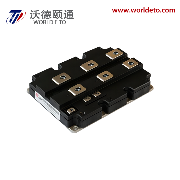
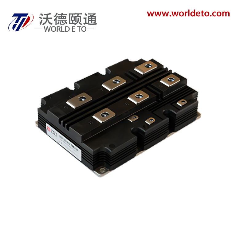
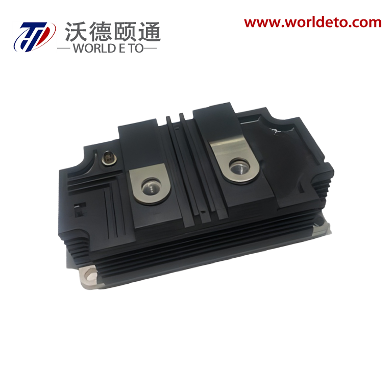
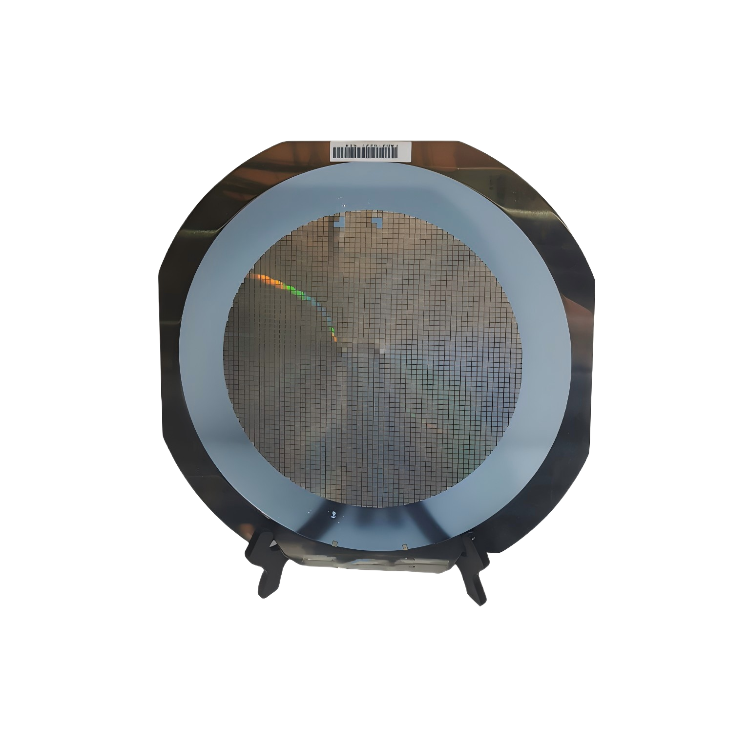
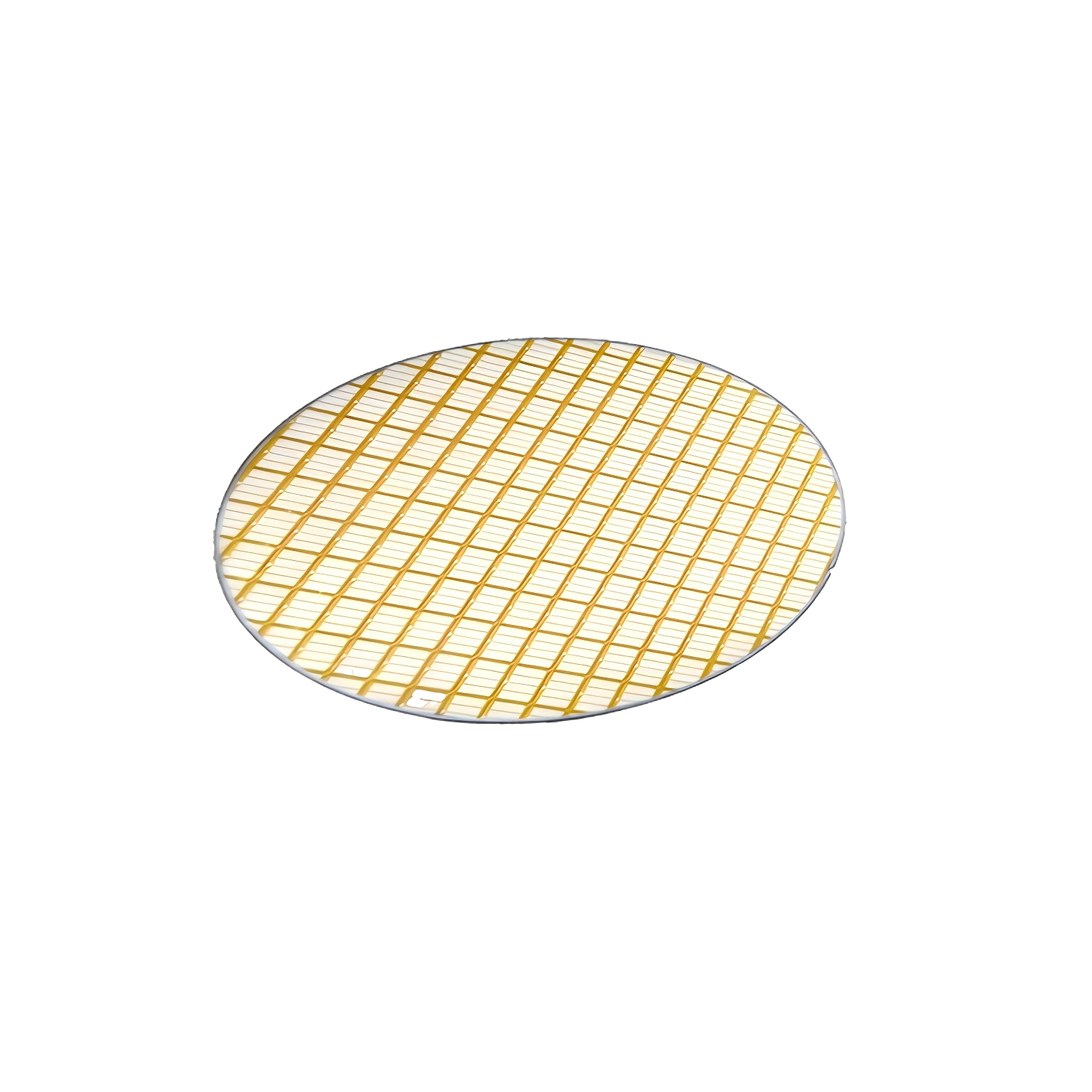
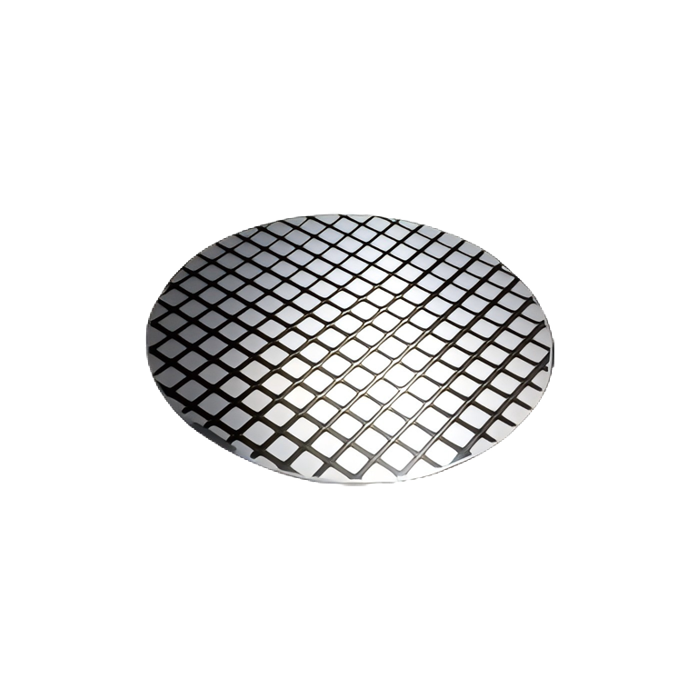
IGBT Wafer Technology: Advanced Power Semiconductors for High-Efficiency Applications

All Categories
Get a Quote

Get a Free Quote

Our representative will contact you soon.
Email
Name
Company Name
Message
0/1000

igbt wafer

The igbt wafer represents a revolutionary semiconductor technology that combines the superior switching characteristics of MOSFETs with the high current capacity of bipolar transistors. This innovative semiconductor substrate forms the foundation for Insulated Gate Bipolar Transistors, which have become essential components in modern power electronics applications. The igbt wafer manufacturing process involves sophisticated techniques including epitaxial growth, ion implantation, and precision lithography to create the complex multilayer structure required for optimal performance. These wafers typically feature a P-N-P-N four-layer structure that enables efficient switching between conducting and blocking states while maintaining excellent thermal stability. The igbt wafer technology incorporates advanced silicon processing methods that result in reduced switching losses, enhanced durability, and improved electrical characteristics compared to traditional power semiconductor solutions. Key technological features include ultra-low saturation voltage, fast switching speeds, and robust short-circuit protection capabilities. The wafer substrate undergoes rigorous quality control measures during production to ensure consistent electrical properties and mechanical integrity. Modern igbt wafer designs incorporate trench gate structures that maximize current density while minimizing conduction losses. The manufacturing process utilizes high-purity silicon substrates with precise dopant concentration control to achieve optimal device characteristics. Applications for igbt wafer technology span across multiple industries including renewable energy systems, electric vehicles, industrial motor drives, and power supply units. The versatile nature of igbt wafer technology makes it suitable for both high-frequency switching applications and high-power conversion systems, providing engineers with flexible design options for various power management requirements.

New Products

The igbt wafer delivers exceptional performance benefits that directly translate to cost savings and improved system reliability for end users. One of the most significant advantages is the dramatic reduction in power losses during switching operations, which can decrease energy consumption by up to thirty percent compared to older semiconductor technologies. This efficiency improvement leads to lower operating costs and reduced heat generation, allowing for smaller cooling systems and more compact equipment designs. The igbt wafer technology enables faster switching frequencies while maintaining stable operation, which results in smaller passive components and reduced overall system size. Engineers benefit from simplified circuit designs because igbt wafer devices combine the voltage control advantages of field-effect transistors with the current handling capabilities of bipolar devices. The robust construction of igbt wafer products ensures reliable operation in harsh industrial environments with temperature fluctuations, voltage spikes, and electromagnetic interference. Manufacturers appreciate the consistent quality and predictable performance characteristics of igbt wafer technology, which reduces production variability and improves yield rates in electronic assembly processes. The enhanced thermal management properties of igbt wafer devices allow for higher power density applications without compromising reliability or lifespan. System designers can achieve better electromagnetic compatibility because igbt wafer switching produces lower electromagnetic emissions compared to alternative technologies. The igbt wafer platform supports both low-voltage and high-voltage applications, providing design flexibility across different power ranges and voltage levels. Maintenance requirements are significantly reduced due to the inherent durability and self-protection features built into igbt wafer technology. The technology offers superior short-circuit protection and overcurrent handling, which prevents catastrophic failures and extends equipment service life. Cost-effectiveness is enhanced through reduced component counts, simplified thermal management, and improved manufacturing yields, making igbt wafer technology an economically attractive solution for power electronics applications.

Practical Tips

Is Your ADC/DAC Underperforming? The Culprit Could Be Your Voltage Reference

24

Nov

Is Your ADC/DAC Underperforming? The Culprit Could Be Your Voltage Reference

In the realm of precision analog-to-digital and digital-to-analog conversion, engineers often focus on the specifications of the ADC or DAC itself while overlooking a critical component that can make or break system performance. The voltage reference...
View More
High-Performance ADC Chips and Precision DACs: Analysis of High-Speed, Low-Power Domestic Alternatives

02

Feb

High-Performance ADC Chips and Precision DACs: Analysis of High-Speed, Low-Power Domestic Alternatives

The semiconductor industry has witnessed unprecedented growth in demand for high-performance analog-to-digital converter chips and precision digital-to-analog converters. As electronic systems become increasingly sophisticated, the need for reliable,...
View More
Super-junction MOSFET

25

Jan

Super-junction MOSFET

The super-junction MOSFET (Meta Oxide Semiconductor Field Effect Transistor) introduces a lateral electric field control on the basis of the traditional VDMOS, thereby making the vertical electric field distribution approach an ideal rectangle. This ...
View More
Precision DAC Chips: Achieving Sub-Millivolt Accuracy in Complex Control Systems

03

Feb

Precision DAC Chips: Achieving Sub-Millivolt Accuracy in Complex Control Systems

Modern industrial control systems demand unprecedented accuracy and reliability, with precision DAC chips serving as critical components that bridge the digital-analog divide. These sophisticated semiconductor devices enable engineers to achieve sub-...
View More

Get a Free Quote

Our representative will contact you soon.
Email
Name
Company Name
Message
0/1000

igbt wafer

Superior Power Efficiency and Energy Savings

Superior Power Efficiency and Energy Savings

The igbt wafer technology revolutionizes power conversion efficiency through its unique semiconductor structure that minimizes energy losses during operation. This advanced wafer design incorporates optimized carrier injection and extraction mechanisms that significantly reduce both conduction and switching losses compared to conventional power devices. The carefully engineered igbt wafer substrate features precise dopant profiles and innovative cell geometries that enable superior carrier mobility and reduced resistance paths. Users experience substantial reductions in electricity costs due to the exceptional efficiency ratings that igbt wafer devices consistently achieve across various operating conditions. The thermal performance characteristics of igbt wafer technology allow for higher current densities while maintaining stable junction temperatures, resulting in more compact system designs with reduced cooling requirements. Industrial applications benefit from the improved power factor and reduced harmonic distortion that igbt wafer devices provide, leading to cleaner power delivery and enhanced system reliability. The igbt wafer platform enables power conversion systems to operate at efficiency levels exceeding ninety-eight percent in many applications, translating to significant energy savings over the equipment lifespan. Environmental benefits are substantial as the reduced power consumption directly correlates to lower carbon emissions and decreased environmental impact. The advanced manufacturing techniques used in igbt wafer production ensure consistent electrical characteristics that maintain efficiency performance throughout the device lifetime. Quality control processes verify that each igbt wafer meets stringent efficiency standards before integration into power electronic systems, guaranteeing reliable performance for end users.
Enhanced Switching Performance and Frequency Capabilities

Enhanced Switching Performance and Frequency Capabilities

The igbt wafer technology delivers breakthrough switching performance that enables higher operating frequencies while maintaining excellent control characteristics and minimal electromagnetic interference. This exceptional switching capability stems from the optimized gate structure and carefully controlled carrier dynamics within the igbt wafer substrate, allowing for precise control of turn-on and turn-off transitions. The advanced igbt wafer design incorporates innovative techniques such as trench gate architectures and optimized buffer layers that significantly reduce switching times and associated losses. Engineers can design more responsive power conversion systems because igbt wafer devices offer superior control bandwidth and faster dynamic response compared to traditional semiconductor solutions. The enhanced switching performance of igbt wafer technology enables the use of higher switching frequencies, which directly results in smaller magnetic components and reduced overall system weight and volume. Power supply designers benefit from the improved transient response and reduced output ripple that igbt wafer switching characteristics provide, leading to better regulation and cleaner output waveforms. The igbt wafer platform supports both hard-switching and soft-switching topologies, giving design engineers flexibility to optimize their circuits for specific performance requirements. Electromagnetic compatibility is significantly improved due to the controlled switching transitions and reduced di/dt and dv/dt rates that igbt wafer devices inherently provide. The technology enables precise deadtime control and synchronized switching operations in multi-device applications, ensuring optimal system performance and reliability. Quality testing procedures verify that each igbt wafer meets strict switching parameter specifications, ensuring consistent performance across production batches and maintaining long-term reliability in demanding applications.
Robust Reliability and Extended Service Life

Robust Reliability and Extended Service Life

The igbt wafer technology establishes new standards for semiconductor reliability through advanced materials science and innovative manufacturing processes that ensure consistent performance under extreme operating conditions. The robust construction of igbt wafer devices incorporates multiple protection mechanisms including thermal shutdown, overcurrent detection, and short-circuit protection that prevent catastrophic failures and extend operational lifespan. Quality assurance protocols during igbt wafer production include comprehensive stress testing, thermal cycling, and accelerated aging procedures that verify device reliability under various environmental conditions. The inherent ruggedness of igbt wafer technology enables operation in harsh industrial environments with temperature fluctuations, voltage transients, and mechanical vibrations without performance degradation. Failure analysis data demonstrates that igbt wafer devices consistently exceed reliability expectations with mean time between failures significantly higher than competing semiconductor technologies. The advanced packaging and interconnection methods used with igbt wafer technology provide superior mechanical stability and thermal cycling resistance, ensuring long-term connection integrity. System maintenance costs are substantially reduced because igbt wafer devices require minimal preventive maintenance and demonstrate predictable performance characteristics throughout their operational life. The technology incorporates self-diagnostic capabilities that enable condition monitoring and predictive maintenance strategies, helping users optimize system uptime and performance. Automotive and aerospace applications particularly benefit from the exceptional reliability standards that igbt wafer technology provides, meeting stringent qualification requirements for safety-critical systems. The comprehensive warranty coverage and technical support available for igbt wafer products provide additional confidence for system designers and end users investing in power electronics solutions.

Get a Free Quote

Our representative will contact you soon.
Email
Name
Company Name
Message
0/1000