8 Inch Wafer: Advanced Semiconductor Substrate Solutions for Manufacturing Excellence

All Categories
Get a Quote

Get a Free Quote

Our representative will contact you soon.
Email
Name
Company Name
Message
0/1000

8 inch wafer

The 8 inch wafer represents a critical component in semiconductor manufacturing, serving as the foundation for producing integrated circuits and electronic devices. This silicon substrate measures precisely 200 millimeters in diameter and has become an industry standard for manufacturing various semiconductor products. The 8 inch wafer functions as a base material where multiple semiconductor devices are fabricated simultaneously through complex photolithography and etching processes. Manufacturing facilities utilize these wafers to create microprocessors, memory chips, power management units, and analog circuits that power everything from smartphones to automotive systems. The technological features of the 8 inch wafer include exceptional purity levels, with silicon content exceeding 99.9999 percent, ensuring optimal electrical properties for semiconductor applications. These wafers undergo rigorous quality control processes to maintain uniform thickness, typically ranging from 525 to 775 micrometers, and achieve extremely flat surfaces with minimal defects. Advanced crystal growth techniques produce wafers with consistent crystalline structure, enabling reliable device performance across the entire surface area. The 8 inch wafer supports various doping processes, allowing manufacturers to modify electrical conductivity for specific applications. Temperature resistance capabilities make these wafers suitable for high-performance processing environments, withstanding temperatures up to 1200 degrees Celsius during fabrication. Applications for the 8 inch wafer span numerous industries, including consumer electronics, automotive semiconductors, industrial automation, telecommunications equipment, and renewable energy systems. Manufacturing facilities prefer these wafers for producing analog and mixed-signal devices, power semiconductors, and specialized chips requiring precise electrical characteristics. The standardized dimensions enable compatibility with existing production equipment, making the 8 inch wafer an efficient choice for established manufacturing lines seeking reliable semiconductor substrate solutions.

New Product Recommendations

The 8 inch wafer delivers exceptional cost-effectiveness compared to smaller substrate alternatives, providing manufacturers with optimal production efficiency while maintaining high-quality standards. Companies benefit from reduced per-unit manufacturing costs because multiple devices can be processed simultaneously on each wafer surface, maximizing throughput and minimizing material waste. The standardized 200-millimeter diameter ensures compatibility with existing production equipment, eliminating expensive retooling requirements and enabling seamless integration into established manufacturing workflows. Production facilities appreciate the mature manufacturing infrastructure surrounding 8 inch wafer technology, which translates to reliable supply chains, proven processing techniques, and extensive technical support resources. Quality consistency represents another significant advantage, as the 8 inch wafer maintains uniform electrical and physical properties across its entire surface area, resulting in predictable device performance and higher yield rates. Manufacturing teams can rely on established process parameters and proven methodologies, reducing development time and accelerating product launch schedules. The balanced size of the 8 inch wafer offers optimal handling characteristics, providing sufficient surface area for multiple devices while remaining manageable for automated processing equipment and human operators. This size advantage eliminates many handling complications associated with larger substrates while delivering better economics than smaller alternatives. Thermal management benefits emerge from the wafer's optimized thickness and diameter ratio, enabling efficient heat dissipation during high-temperature processing steps and improving overall device reliability. Supply chain advantages include widespread availability from multiple suppliers, competitive pricing due to established production volumes, and reduced lead times compared to specialized substrate sizes. The 8 inch wafer supports diverse applications ranging from simple analog circuits to complex mixed-signal devices, providing manufacturers with flexibility to address various market segments using standardized production processes. Environmental considerations favor the 8 inch wafer through optimized material utilization, reduced chemical consumption per device, and lower energy requirements during processing, contributing to sustainable manufacturing practices while maintaining profitability.

Tips And Tricks

How to Choose a Precision DAC: A Guide to Critical Specs and Top Domestic Models

24

Nov

How to Choose a Precision DAC: A Guide to Critical Specs and Top Domestic Models

In today's rapidly evolving electronics landscape, selecting the right precision DAC has become increasingly critical for engineers developing high-performance systems. A precision DAC serves as the crucial bridge between digital control systems and ...
View More
Is Your ADC/DAC Underperforming? The Culprit Could Be Your Voltage Reference

24

Nov

Is Your ADC/DAC Underperforming? The Culprit Could Be Your Voltage Reference

In the realm of precision analog-to-digital and digital-to-analog conversion, engineers often focus on the specifications of the ADC or DAC itself while overlooking a critical component that can make or break system performance. The voltage reference...
View More
From ADC to LDO: Complete High-Precision, Low-Power Domestic Chip Replacement Solutions

02

Feb

From ADC to LDO: Complete High-Precision, Low-Power Domestic Chip Replacement Solutions

The semiconductor industry faces unprecedented challenges as global supply chain disruptions and geopolitical tensions drive demand for reliable domestic chip replacement solutions. Companies across industries are increasingly seeking alternatives to...
View More
The Best Domestic Alternatives for High-Performance ADC and DAC Chips in 2026

03

Feb

The Best Domestic Alternatives for High-Performance ADC and DAC Chips in 2026

The semiconductor industry is experiencing unprecedented demand for high-performance analog-to-digital converter and digital-to-analog converter solutions, driving engineers and procurement teams to seek reliable domestic alternatives for ADC and DAC...
View More

Get a Free Quote

Our representative will contact you soon.
Email
Name
Company Name
Message
0/1000

8 inch wafer

Superior Manufacturing Efficiency and Cost Optimization

Superior Manufacturing Efficiency and Cost Optimization

The 8 inch wafer excels in manufacturing efficiency through its optimal balance of surface area and handling characteristics, delivering substantial cost savings for semiconductor production facilities. This carefully engineered substrate size allows manufacturers to process significantly more devices per wafer compared to smaller alternatives, directly translating into reduced per-unit production costs and improved profit margins. Production teams benefit from the wafer's standardized dimensions, which enable precise automation and consistent processing parameters across multiple manufacturing runs. The 200-millimeter diameter provides ample space for complex circuit layouts while maintaining compatibility with established production equipment, eliminating costly infrastructure upgrades. Manufacturing efficiency gains emerge from reduced setup times, streamlined material handling procedures, and optimized chemical usage during processing steps. Quality control processes become more effective with the 8 inch wafer because inspection equipment can evaluate larger areas efficiently, identifying potential defects early in the production cycle. Yield optimization strategies work particularly well with this substrate size, as manufacturers can implement statistical process control methods across multiple device sites simultaneously. The mature ecosystem surrounding 8 inch wafer technology includes extensive supplier networks, proven processing recipes, and comprehensive technical documentation, reducing development costs and accelerating time-to-market for new products. Energy efficiency improvements result from optimized processing chamber utilization, where the wafer size maximizes equipment capacity without exceeding thermal or mechanical limits. Waste reduction benefits include minimized edge exclusion zones, improved chemical utilization rates, and reduced packaging materials per finished device. Long-term cost advantages extend beyond initial manufacturing savings to include reduced maintenance requirements, lower training costs for operators, and simplified inventory management procedures. The established supply chain infrastructure ensures competitive pricing, reliable availability, and consistent quality standards that support predictable production planning and financial forecasting.
Exceptional Quality and Reliability Standards

Exceptional Quality and Reliability Standards

The 8 inch wafer maintains exceptional quality standards through rigorous manufacturing processes that ensure consistent electrical and physical properties essential for reliable semiconductor device performance. Advanced crystal growth techniques produce wafers with uniform crystalline structure, minimizing defects and variations that could compromise device functionality or yield rates. Quality control measures include comprehensive surface inspection, electrical characterization, and dimensional verification to guarantee each wafer meets stringent industry specifications before reaching production facilities. The substrate's inherent stability results from optimized silicon purification processes that achieve contamination levels below one part per billion, ensuring predictable electrical behavior across diverse operating conditions. Thermal stability characteristics enable the 8 inch wafer to withstand extreme processing temperatures without warping, cracking, or developing stress-related defects that could affect device performance. Mechanical properties include carefully controlled thickness uniformity, typically maintained within plus or minus 5 micrometers across the entire wafer surface, supporting precise photolithography and etching operations. Surface flatness specifications ensure optimal contact between photoresist materials and substrate, enabling accurate pattern transfer for fine-geometry features. The wafer's electrical properties remain consistent across its diameter, with resistivity variations held to minimal levels that support uniform device characteristics. Contamination control protocols during manufacturing prevent metallic and organic impurities from compromising substrate integrity, maintaining the pristine conditions necessary for high-performance semiconductor applications. Reliability testing includes accelerated aging studies, thermal cycling evaluations, and mechanical stress assessments that validate long-term stability under operating conditions. Documentation systems track each wafer's manufacturing history, processing parameters, and quality metrics, enabling traceability and continuous improvement initiatives. The established quality infrastructure surrounding 8 inch wafer production includes certified suppliers, standardized testing procedures, and comprehensive quality management systems that ensure consistent performance across different manufacturing locations and time periods.
Versatile Applications and Industry Compatibility

Versatile Applications and Industry Compatibility

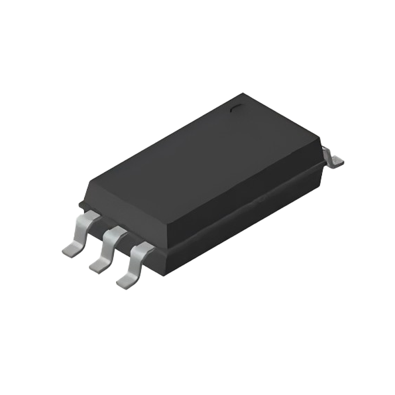
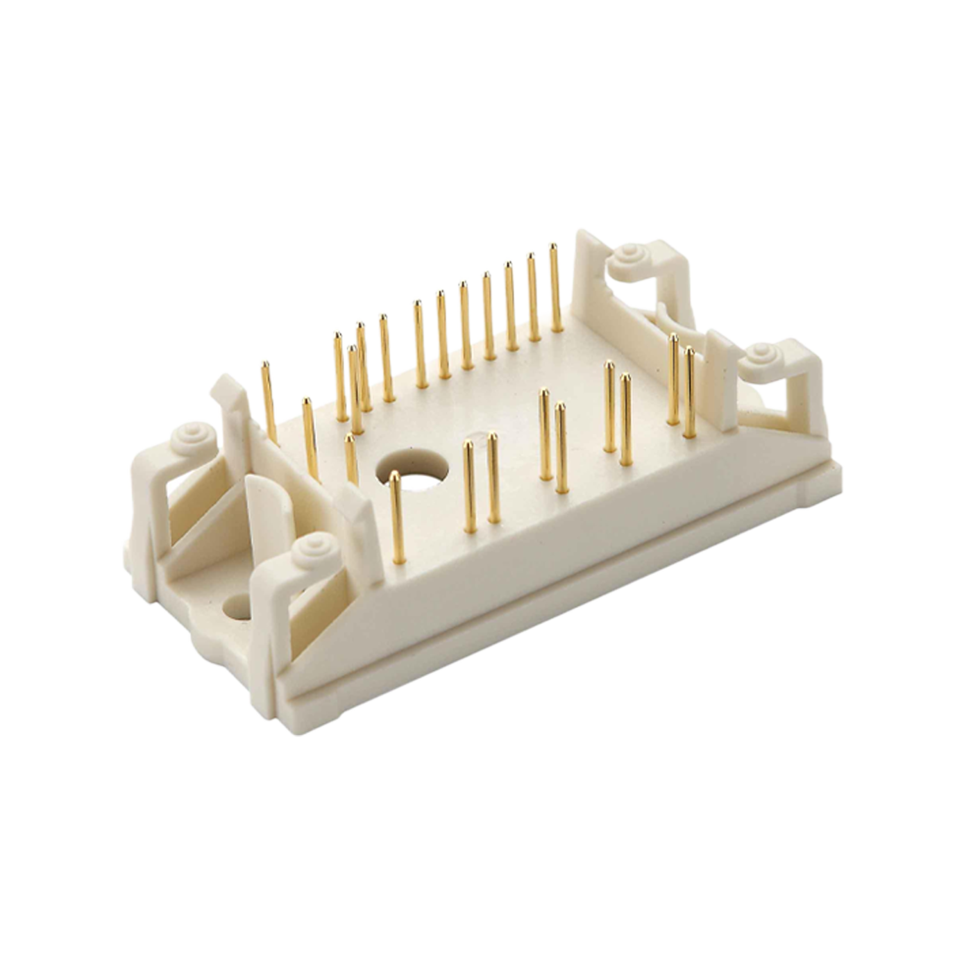
The 8 inch wafer demonstrates remarkable versatility across multiple industry sectors, supporting diverse applications from consumer electronics to automotive systems through its adaptable processing capabilities and standardized specifications. This substrate excels in power semiconductor manufacturing, where its thermal properties and size characteristics enable efficient production of devices handling high currents and voltages. Automotive applications benefit from the wafer's reliability standards and proven manufacturing processes, supporting critical systems like engine control units, safety systems, and electric vehicle power management. Consumer electronics manufacturers utilize the 8 inch wafer for analog and mixed-signal devices, taking advantage of its cost-effectiveness and mature processing techniques to deliver affordable products with consistent performance. Industrial automation applications leverage the wafer's robust characteristics for sensor interfaces, motor control circuits, and communication modules that operate in demanding environments. The substrate's compatibility with various doping processes enables manufacturers to create devices with precisely tailored electrical characteristics, supporting both high-speed digital applications and sensitive analog circuits. Radio frequency applications benefit from the wafer's low noise characteristics and uniform electrical properties, enabling production of wireless communication components with predictable performance. Renewable energy systems utilize devices manufactured on 8 inch wafers for solar inverters, wind turbine controllers, and energy storage management systems, taking advantage of the substrate's reliability and cost-effectiveness. Medical electronics applications rely on the wafer's quality standards and biocompatibility for implantable devices, diagnostic equipment, and monitoring systems requiring long-term stability. The established ecosystem includes specialized processing equipment, materials suppliers, and technical expertise specifically optimized for 8 inch wafer applications. Flexibility extends to packaging options, testing procedures, and assembly techniques that accommodate diverse end-user requirements. Market acceptance across multiple industries creates economies of scale that benefit all users through reduced costs, improved availability, and continuous technology improvements. Future applications continue expanding as manufacturers discover new ways to leverage the 8 inch wafer's balanced characteristics for emerging technologies and market opportunities.

Get a Free Quote

Our representative will contact you soon.
Email
Name
Company Name
Message
0/1000