Advanced Power Wafer Fabrication Solutions - High-Performance Semiconductor Substrates

All Categories
Get a Quote

Get a Free Quote

Our representative will contact you soon.
Email
Name
Company Name
Message
0/1000

power wafer fabrication

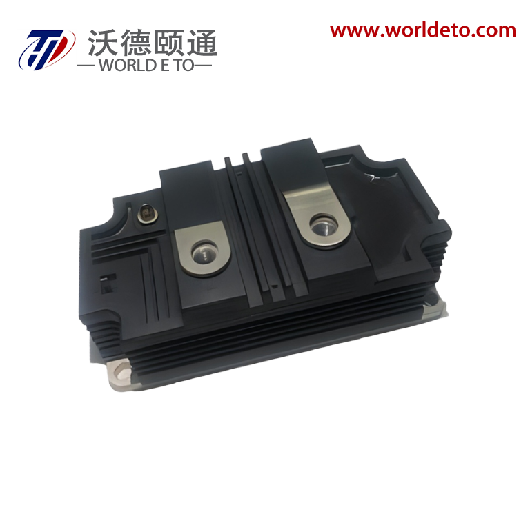
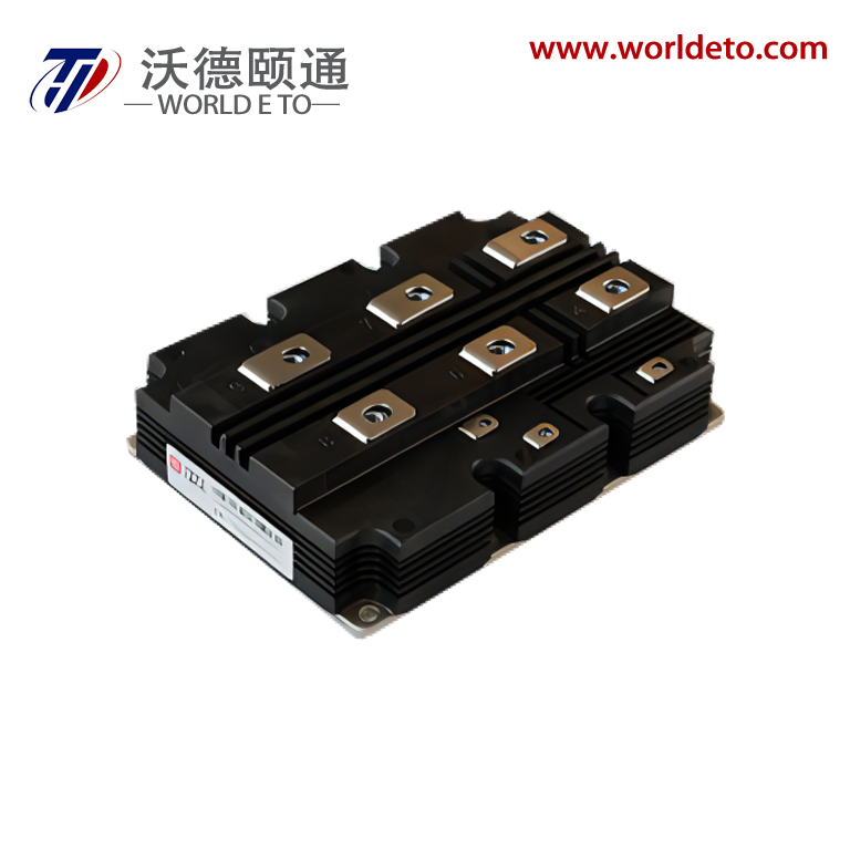
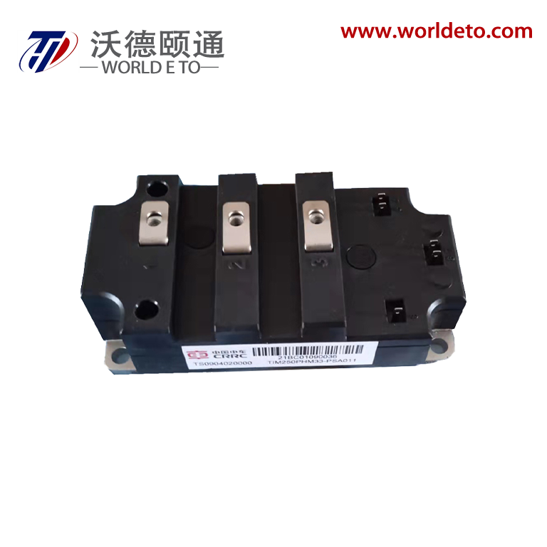
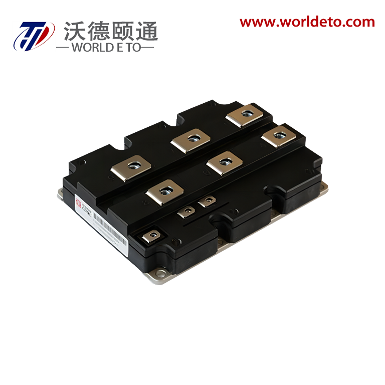
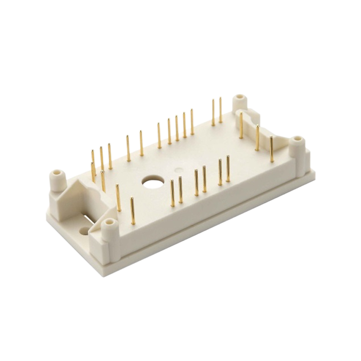
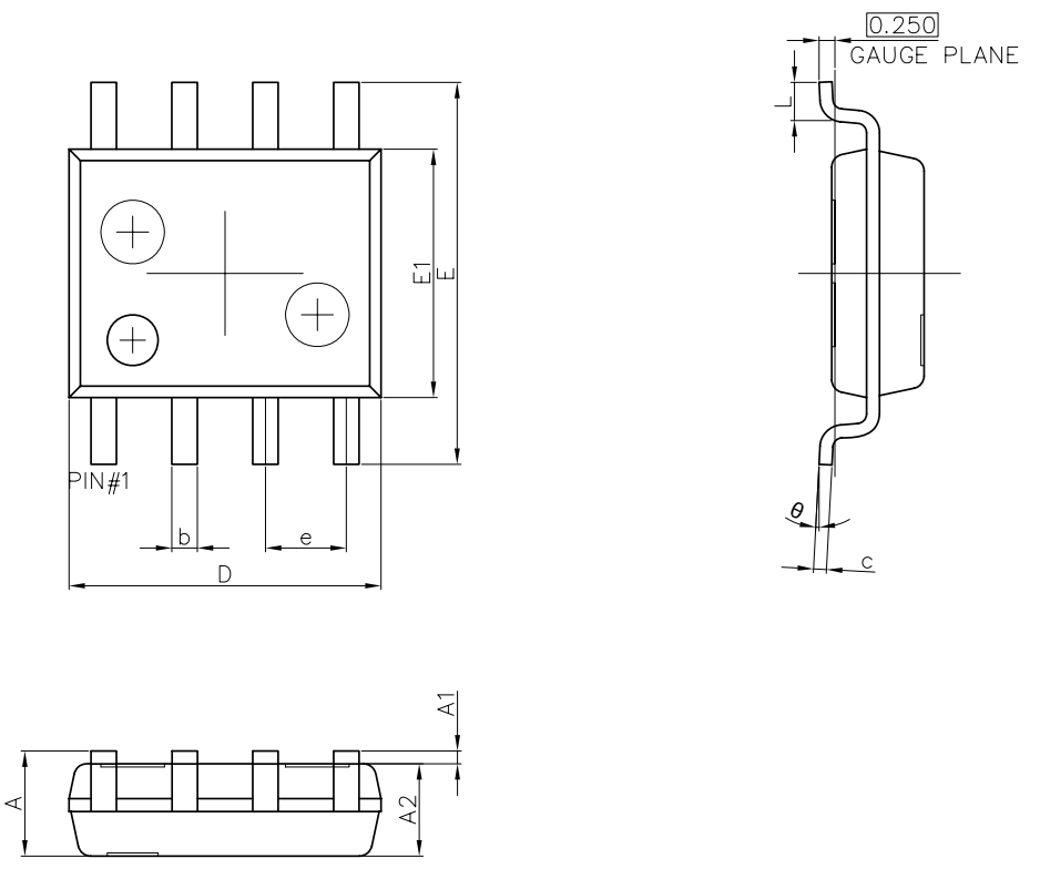
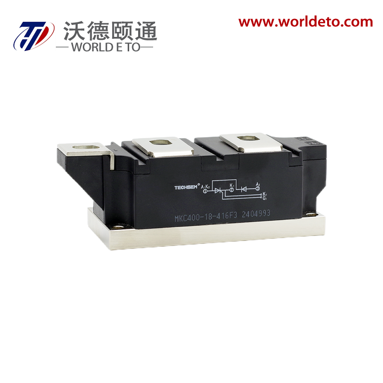
Power wafer fabrication represents a sophisticated semiconductor manufacturing process that creates specialized silicon wafers designed for high-power electronic applications. This advanced technology transforms raw silicon materials into precision-engineered substrates that serve as the foundation for power semiconductor devices. The power wafer fabrication process involves multiple complex stages, including crystal growth, wafer slicing, surface preparation, and quality control procedures that ensure optimal performance characteristics. These manufactured wafers exhibit superior electrical properties, enhanced thermal conductivity, and exceptional structural integrity compared to standard semiconductor wafers. The main functions of power wafer fabrication encompass the production of substrates for power MOSFETs, IGBTs, diodes, and other high-voltage semiconductor components used in electric vehicles, renewable energy systems, and industrial automation equipment. Technological features include precise dopant concentration control, advanced crystal orientation techniques, and specialized surface treatments that optimize carrier mobility and reduce electrical losses. The fabrication process utilizes state-of-the-art cleanroom environments, automated handling systems, and rigorous testing protocols to maintain consistent quality standards. Applications span across automotive electronics, power conversion systems, motor drives, and grid-tied inverters where reliable performance under extreme operating conditions is essential. Modern power wafer fabrication techniques incorporate innovative materials science approaches, including silicon carbide and gallium nitride alternatives for next-generation power devices. The manufacturing process requires specialized equipment capable of handling larger wafer diameters and thicker substrates while maintaining tight dimensional tolerances and surface quality specifications that meet demanding industry requirements for power semiconductor applications.

New Product Releases

Power wafer fabrication delivers exceptional performance benefits that directly translate into superior product reliability and operational efficiency for manufacturers and end-users alike. The advanced manufacturing processes create wafers with enhanced electrical characteristics that enable power devices to handle higher current densities and voltage levels while maintaining optimal thermal management properties. This improved performance capability allows engineers to design more compact and efficient power systems that consume less energy and generate reduced heat output during operation. The precision manufacturing techniques used in power wafer fabrication result in consistent material properties across entire wafer surfaces, eliminating performance variations that can compromise device reliability in critical applications. Manufacturers benefit from higher production yields due to the superior quality control measures implemented throughout the fabrication process, which reduces waste and lowers overall manufacturing costs. The enhanced substrate quality enables power devices to achieve longer operational lifespans, reducing maintenance requirements and replacement costs for end-users in automotive, industrial, and renewable energy applications. Power wafer fabrication processes incorporate advanced dopant control methods that create uniform electrical properties, enabling predictable device behavior and simplified circuit design procedures for engineering teams. The improved thermal conductivity characteristics of fabricated power wafers allow for more effective heat dissipation, enabling higher power density designs without compromising reliability or safety margins. Cost-effectiveness emerges through reduced material waste, optimized processing parameters, and scalable production methods that accommodate varying volume requirements while maintaining consistent quality standards. The manufacturing flexibility inherent in modern power wafer fabrication allows for rapid customization of substrate specifications to meet specific application requirements without extensive retooling or process modifications. Environmental benefits include reduced energy consumption during device operation, lower material waste generation, and compatibility with sustainable manufacturing practices that align with corporate environmental responsibility initiatives.

Practical Tips

Achieving Peak Performance: How High-Speed ADCs and Precision Amplifiers Work Together

07

Jan

Achieving Peak Performance: How High-Speed ADCs and Precision Amplifiers Work Together

In today's rapidly evolving electronics landscape, the demand for precise and rapid signal processing continues to grow exponentially. From telecommunications infrastructure to advanced measurement systems, engineers are constantly seeking solutions ...
View More
High-Accuracy ADC & DAC Chips: The Core of Precision Measurement Systems

07

Jan

High-Accuracy ADC & DAC Chips: The Core of Precision Measurement Systems

In today's advanced measurement and control systems, the bridge between analog real-world signals and digital processing relies heavily on specialized semiconductor components. These critical interface chips, specifically High-Accuracy ADC & DAC Chip...
View More
Low-Power, High-Precision: How Domestic Linear Regulators and Voltage References Enable Import Substitution

02

Feb

Low-Power, High-Precision: How Domestic Linear Regulators and Voltage References Enable Import Substitution

The global semiconductor supply chain disruptions of recent years have highlighted the critical importance of developing robust domestic manufacturing capabilities. As industries worldwide grapple with component shortages and geopolitical tensions, t...
View More
High-Precision ADC, DAC, and Voltage References: Comprehensive Analysis of Low-Power Domestic Solutions

02

Feb

High-Precision ADC, DAC, and Voltage References: Comprehensive Analysis of Low-Power Domestic Solutions

The demand for high-precision analog-to-digital converters in modern electronic systems continues to surge as industries require increasingly accurate measurement and control capabilities. High-precision ADC technology forms the backbone of sophistic...
View More

Get a Free Quote

Our representative will contact you soon.
Email
Name
Company Name
Message
0/1000

power wafer fabrication

Advanced Crystal Structure Engineering

Advanced Crystal Structure Engineering

Power wafer fabrication employs sophisticated crystal structure engineering techniques that fundamentally transform the electrical and mechanical properties of silicon substrates to meet demanding power application requirements. The process begins with carefully controlled crystal growth procedures that establish optimal lattice structures with minimal defect densities, creating the foundation for superior device performance. Advanced Czochralski pulling methods combined with precise temperature gradients ensure uniform crystal orientation throughout the entire wafer diameter, eliminating structural inconsistencies that could compromise electrical conductivity or mechanical strength. The engineering process incorporates strategic dopant introduction at controlled concentrations to achieve specific resistivity profiles that optimize current-carrying capacity while maintaining voltage blocking capabilities essential for power device operation. Specialized annealing procedures remove residual stress patterns and stabilize crystal structures, resulting in improved long-term reliability under thermal cycling conditions common in automotive and industrial applications. The crystal engineering approach enables precise control over carrier mobility characteristics, allowing power devices manufactured on these substrates to achieve faster switching speeds and reduced conduction losses compared to conventional alternatives. Quality assurance procedures include comprehensive crystallographic analysis using X-ray diffraction techniques and electrical characterization methods that verify structural integrity and electrical properties meet stringent specifications. The advanced engineering methods create substrates with enhanced mechanical strength that resist cracking and warping during subsequent device processing steps, improving manufacturing yield rates and reducing production costs. Temperature coefficient optimization through crystal structure modification ensures stable electrical performance across wide operating temperature ranges, critical for automotive electronics and outdoor power conversion equipment. The engineering precision achieved through these advanced methods enables power semiconductor manufacturers to develop next-generation devices with improved efficiency ratings and enhanced reliability characteristics that exceed industry standards for demanding applications requiring consistent performance under extreme operating conditions.
Superior Thermal Management Properties

Superior Thermal Management Properties

Power wafer fabrication incorporates specialized techniques that significantly enhance thermal management properties, creating substrates with exceptional heat dissipation capabilities essential for high-power semiconductor applications. The manufacturing process optimizes thermal conductivity through controlled crystal structure modifications and surface treatments that facilitate efficient heat transfer from active device regions to heat sink assemblies. Advanced substrate preparation methods create microscopic surface textures that maximize thermal interface contact area while maintaining electrical isolation properties required for safe operation in high-voltage applications. The enhanced thermal properties result from carefully engineered material compositions that balance electrical performance requirements with superior heat conduction characteristics, enabling power devices to operate at higher current densities without exceeding safe junction temperatures. Specialized thermal interface optimization reduces thermal resistance between semiconductor junctions and substrate surfaces, improving overall system thermal efficiency and enabling more compact power module designs. The fabrication process incorporates thermal stress relief techniques that prevent substrate cracking or delamination during temperature cycling, ensuring long-term reliability in automotive and industrial applications where thermal cycling is common. Quality control procedures include comprehensive thermal characterization using advanced metrology equipment that verifies thermal conductivity values and thermal expansion coefficients meet specification requirements for specific applications. The superior thermal management capabilities enable power system designers to achieve higher power densities while maintaining safe operating temperatures, reducing cooling system requirements and overall system costs. Thermal modeling compatibility ensures that fabricated substrates provide predictable thermal behavior for accurate thermal simulation during power module design phases, reducing development time and improving design optimization. The enhanced thermal properties contribute to improved device efficiency by reducing temperature-dependent losses and enabling operation at optimal performance points across wider temperature ranges. Environmental benefits include reduced cooling energy requirements and improved system reliability that extends operational lifespans, contributing to sustainable technology solutions for renewable energy and electric vehicle applications.
Precision Quality Control Systems

Precision Quality Control Systems

Power wafer fabrication implements comprehensive precision quality control systems that ensure consistent substrate performance and reliability across all production batches through rigorous testing and measurement protocols. The quality control framework incorporates multiple inspection stages throughout the manufacturing process, beginning with incoming raw material verification and extending through final substrate characterization and packaging procedures. Advanced metrology equipment performs detailed surface analysis using atomic force microscopy and scanning electron microscopy techniques to detect microscopic defects that could compromise device performance or reliability. Electrical characterization procedures include comprehensive resistivity mapping, carrier lifetime measurements, and minority carrier diffusion length analysis that verify electrical properties meet stringent specifications for power semiconductor applications. The precision control systems utilize statistical process control methods that monitor key process parameters in real-time, enabling immediate corrective actions when variations exceed predetermined control limits. Automated inspection systems perform non-destructive testing procedures that evaluate crystal quality, surface contamination levels, and dimensional accuracy without compromising substrate integrity or introducing handling damage. Comprehensive documentation systems maintain detailed traceability records for each substrate, enabling rapid identification and resolution of quality issues while providing valuable feedback for continuous process improvement initiatives. The quality control protocols include accelerated aging tests and thermal cycling evaluations that predict long-term reliability performance under actual operating conditions, ensuring substrates meet durability requirements for automotive and industrial applications. Precision measurement capabilities extend to sub-micron dimensional tolerances and parts-per-billion contamination detection levels, exceeding industry standards for semiconductor substrate quality. Calibrated measurement equipment undergoes regular verification procedures using certified reference standards to maintain measurement accuracy and traceability to national measurement institutes. The comprehensive quality systems enable rapid identification of process variations and implementation of corrective measures that maintain consistent product quality while optimizing manufacturing efficiency and reducing production costs through improved yield rates and reduced rework requirements.

Get a Free Quote

Our representative will contact you soon.
Email
Name
Company Name
Message
0/1000