MOSFET Die Technology: High-Performance Semiconductor Solutions for Power Electronics

All Categories
Get a Quote

Get a Free Quote

Our representative will contact you soon.
Email
Name
Company Name
Message
0/1000

mosfet die

The mosfet die represents the core semiconductor component that forms the foundation of modern power electronics and switching applications. This miniature silicon wafer contains the essential transistor structure that enables precise control of electrical current flow through voltage-controlled switching mechanisms. The mosfet die operates as a voltage-controlled device where gate voltage determines the conductivity between drain and source terminals, making it fundamental for power management systems across countless electronic devices. Manufacturing processes create these semiconductor structures through advanced photolithography and ion implantation techniques on silicon substrates. The mosfet die architecture incorporates multiple layers including gate oxide, polysilicon gates, and doped silicon regions that work together to achieve efficient switching performance. Temperature characteristics of the mosfet die enable reliable operation across wide thermal ranges, making them suitable for automotive, industrial, and consumer applications. Power handling capabilities vary significantly based on die size and design parameters, with larger dies typically supporting higher current ratings. The mosfet die structure includes built-in body diodes that provide reverse current conduction paths during switching transitions. Advanced packaging techniques protect the mosfet die while providing thermal and electrical connections to external circuits. Quality control measures during production ensure consistent electrical parameters and long-term reliability. The mosfet die technology continues evolving with new materials like silicon carbide and gallium nitride offering superior performance characteristics. Integration capabilities allow multiple mosfet die structures on single substrates, creating complex power management solutions. Testing procedures verify electrical specifications including threshold voltage, on-resistance, and breakdown voltage parameters before final assembly.

New Product Releases

The mosfet die delivers exceptional switching speed that significantly outperforms traditional bipolar transistors in high-frequency applications. This rapid switching capability reduces power losses during transitions, improving overall system efficiency and reducing heat generation. Users benefit from lower operating temperatures and extended component lifespans when incorporating mosfet die technology into their designs. The voltage-controlled operation of the mosfet die requires minimal gate current, making it ideal for battery-powered applications where power consumption matters. This characteristic enables direct interfacing with microcontrollers and digital logic circuits without requiring additional driver circuits in many cases. Manufacturing consistency ensures that each mosfet die meets strict quality standards, providing reliable performance across production batches. This consistency reduces design risks and simplifies component selection processes for engineers developing new products. The mosfet die structure inherently provides excellent linearity in its operating region, making it suitable for analog applications requiring precise signal amplification. Thermal performance advantages become apparent in high-power applications where heat dissipation critically affects system reliability. The positive temperature coefficient of resistance in mosfet die technology helps prevent thermal runaway conditions that plague other semiconductor technologies. Packaging flexibility allows mosfet die integration into various form factors, from surface-mount packages for compact designs to high-power modules for industrial applications. Cost-effectiveness emerges from mature manufacturing processes that deliver high-performance mosfet die at competitive prices. The robust nature of mosfet die technology withstands electrical stress and environmental conditions better than many alternative switching solutions. Parallel operation capabilities enable current sharing among multiple mosfet die units, supporting scalable power system designs. Low input capacitance characteristics reduce driving requirements and enable faster switching transitions. The mosfet die technology supports both enhancement and depletion mode operations, providing design flexibility for various circuit topologies. Integration possibilities include incorporating additional features like protection circuits and sensing elements within the same mosfet die structure.

Tips And Tricks

How to Choose a Precision DAC: A Guide to Critical Specs and Top Domestic Models

24

Nov

How to Choose a Precision DAC: A Guide to Critical Specs and Top Domestic Models

In today's rapidly evolving electronics landscape, selecting the right precision DAC has become increasingly critical for engineers developing high-performance systems. A precision DAC serves as the crucial bridge between digital control systems and ...
View More
Is Your ADC/DAC Underperforming? The Culprit Could Be Your Voltage Reference

24

Nov

Is Your ADC/DAC Underperforming? The Culprit Could Be Your Voltage Reference

In the realm of precision analog-to-digital and digital-to-analog conversion, engineers often focus on the specifications of the ADC or DAC itself while overlooking a critical component that can make or break system performance. The voltage reference...
View More
Building Reliable Systems: The Role of Precision Voltage References and LDOs in Industrial Applications

07

Jan

Building Reliable Systems: The Role of Precision Voltage References and LDOs in Industrial Applications

Industrial automation and control systems demand unwavering accuracy and reliability to ensure optimal performance across diverse operating conditions. At the heart of these sophisticated systems lie critical components that provide stable power mana...
View More
Domestic High-Precision Linear Regulators and Instrumentation Amplifiers: Low-Power Design for Replacing Imported Chips

02

Feb

Domestic High-Precision Linear Regulators and Instrumentation Amplifiers: Low-Power Design for Replacing Imported Chips

The semiconductor industry has witnessed a significant shift toward domestically manufactured components, particularly in the realm of precision analog circuits. Domestic high-precision linear regulators have emerged as crucial components for enginee...
View More

Get a Free Quote

Our representative will contact you soon.
Email
Name
Company Name
Message
0/1000

mosfet die

Superior Switching Performance and Efficiency

Superior Switching Performance and Efficiency

The mosfet die technology delivers unmatched switching performance that revolutionizes power conversion efficiency across multiple applications. This exceptional capability stems from the fundamental design of the mosfet die structure, which eliminates minority carrier storage effects that typically slow down switching transitions in bipolar devices. The mosfet die achieves switching times measured in nanoseconds, enabling operation at frequencies exceeding several megahertz while maintaining stable performance characteristics. This high-frequency capability translates directly into smaller passive component requirements, reducing overall system size and cost. Engineers designing power supplies particularly benefit from this feature, as higher switching frequencies allow the use of smaller inductors and capacitors while achieving the same filtering performance. The mosfet die structure incorporates optimized gate oxide thickness and channel geometry that minimize switching losses during both turn-on and turn-off transitions. Advanced manufacturing techniques create mosfet die with reduced parasitic capacitances that further enhance switching speed performance. The resulting efficiency improvements often exceed 95% in well-designed switching circuits, significantly reducing heat generation and cooling requirements. This efficiency advantage becomes increasingly important in battery-powered applications where extended operation time directly correlates with user satisfaction. The mosfet die technology enables soft-switching techniques that further reduce electromagnetic interference and switching losses. Temperature stability of switching characteristics ensures consistent performance across wide operating ranges, making mosfet die suitable for automotive and industrial environments. The low on-resistance characteristics of modern mosfet die minimize conduction losses, complementing the reduced switching losses to achieve overall system efficiency improvements. Quality control measures during mosfet die production ensure consistent switching parameters across manufacturing batches, reducing design margins and improving predictable performance.
Exceptional Thermal Management and Reliability

Exceptional Thermal Management and Reliability

The thermal characteristics of mosfet die technology provide unprecedented reliability and performance stability in demanding applications where temperature control critically affects system operation. Unlike bipolar transistors that suffer from thermal runaway conditions, the mosfet die exhibits a positive temperature coefficient of resistance that naturally limits current flow as temperature increases. This inherent thermal stability prevents catastrophic failures and extends operational lifespan significantly. The silicon substrate of the mosfet die efficiently conducts heat away from active regions, distributing thermal energy across the die structure to prevent localized hot spots. Advanced packaging techniques specifically designed for mosfet die applications enhance thermal dissipation through direct substrate mounting and advanced thermal interface materials. The mosfet die structure tolerates junction temperatures exceeding 175 degrees Celsius while maintaining stable electrical characteristics, making it suitable for automotive and industrial applications with harsh thermal environments. Thermal cycling resistance ensures that repeated heating and cooling cycles do not degrade mosfet die performance or reliability over time. The compact size of mosfet die structures concentrates heat generation in small areas, but advanced thermal modeling and package design effectively manage heat removal. Power derating curves provide clear guidance for maintaining optimal mosfet die performance across temperature ranges, enabling reliable system design. The absence of secondary breakdown effects in mosfet die technology eliminates a major failure mode present in bipolar devices, significantly improving system reliability. Thermal resistance specifications help engineers select appropriate heat sinking and cooling solutions for specific mosfet die applications. Advanced simulation tools accurately predict thermal behavior of mosfet die in complex systems, reducing design iterations and development time. The robust construction of mosfet die withstands thermal shock and rapid temperature changes better than alternative switching technologies. Quality assurance testing includes thermal cycling and high-temperature operation tests that ensure each mosfet die meets stringent reliability requirements before shipment to customers.
Versatile Integration and Design Flexibility

Versatile Integration and Design Flexibility

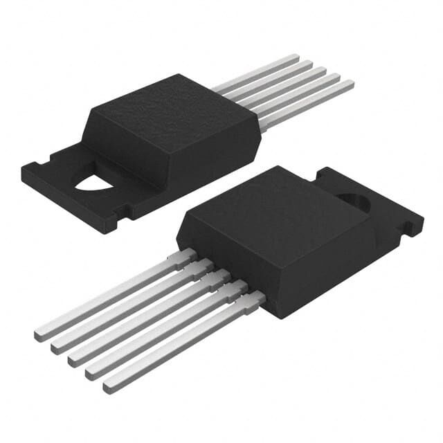
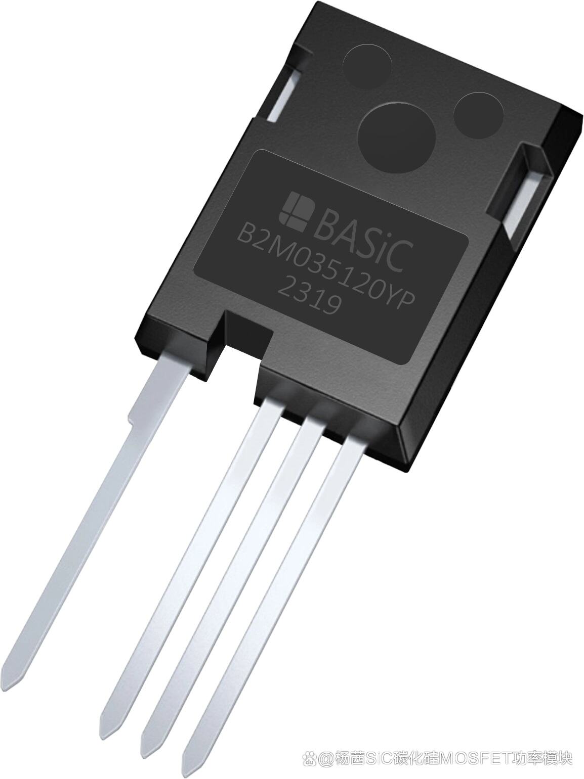
The mosfet die architecture offers exceptional integration capabilities and design flexibility that enable innovative solutions across diverse application requirements. Modern semiconductor fabrication techniques allow multiple mosfet die structures on single substrates, creating integrated power management solutions that reduce component count and board space requirements. This integration capability extends to incorporating additional functionality like gate drivers, protection circuits, and current sensing elements within the same mosfet die package. The scalable nature of mosfet die technology supports both low-power applications requiring minimal switching current and high-power systems handling hundreds of amperes. Parallel operation of multiple mosfet die units enables current sharing and redundancy, improving system reliability and power handling capability. The mosfet die structure adapts to various voltage requirements through optimized design parameters, supporting applications from low-voltage digital circuits to high-voltage power conversion systems. Advanced packaging options accommodate different mechanical and thermal requirements, from ultra-compact surface-mount packages to high-power modules with integrated heat sinks. The mosfet die technology supports both N-channel and P-channel configurations, enabling complementary designs and bridge circuits that simplify power conversion topologies. Gate drive compatibility with standard logic levels eliminates the need for specialized driver circuits in many applications, reducing system complexity and cost. The mosfet die structure inherently provides bidirectional current capability through its body diode, supporting synchronous rectification and energy recovery applications. Customization options include optimized mosfet die designs for specific applications, balancing parameters like on-resistance, switching speed, and voltage rating to meet exact requirements. The mature manufacturing infrastructure for mosfet die ensures reliable supply chains and consistent availability for high-volume production applications. Testing and qualification procedures verify that each mosfet die meets application-specific requirements, providing confidence in performance and reliability. The continuous evolution of mosfet die technology incorporates new materials and structures that further enhance performance and expand application possibilities.

Get a Free Quote

Our representative will contact you soon.
Email
Name
Company Name
Message
0/1000