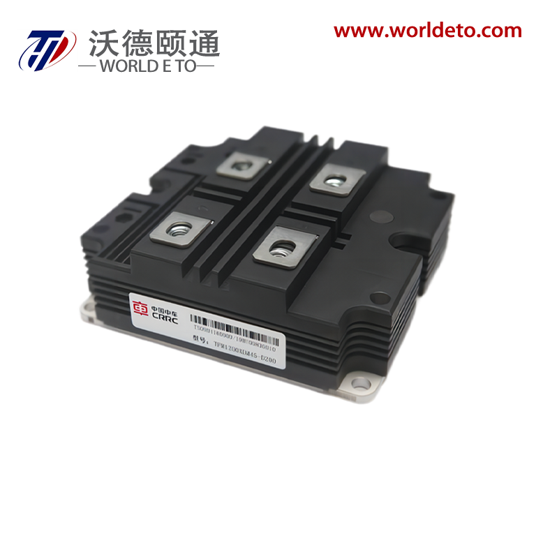
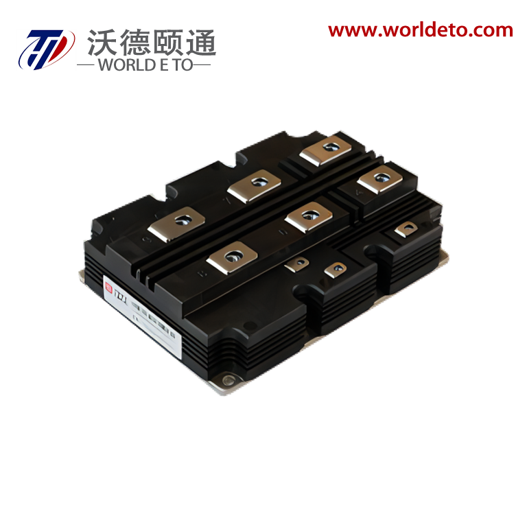
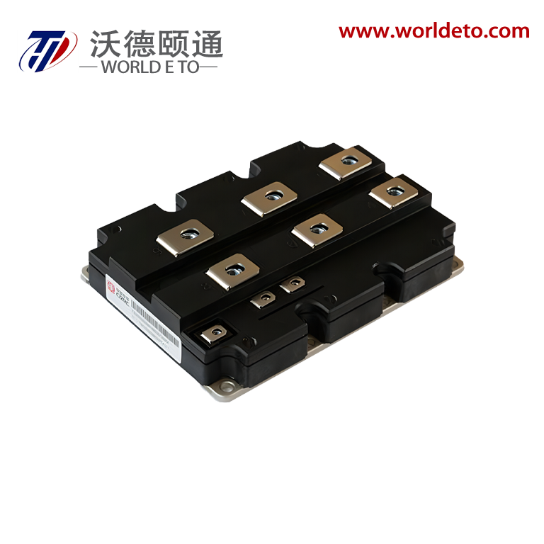
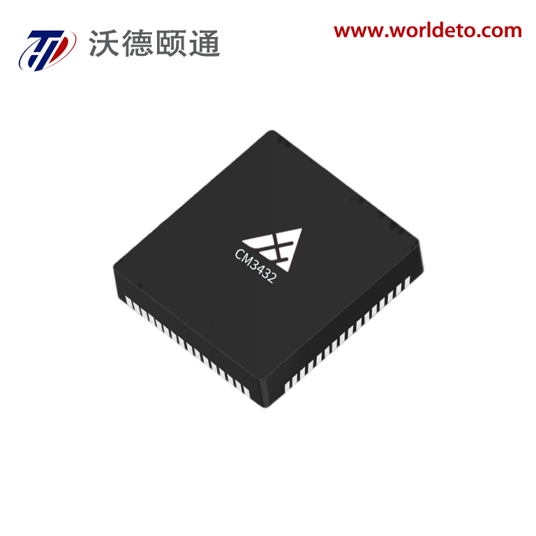
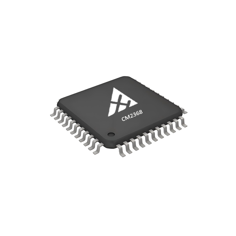
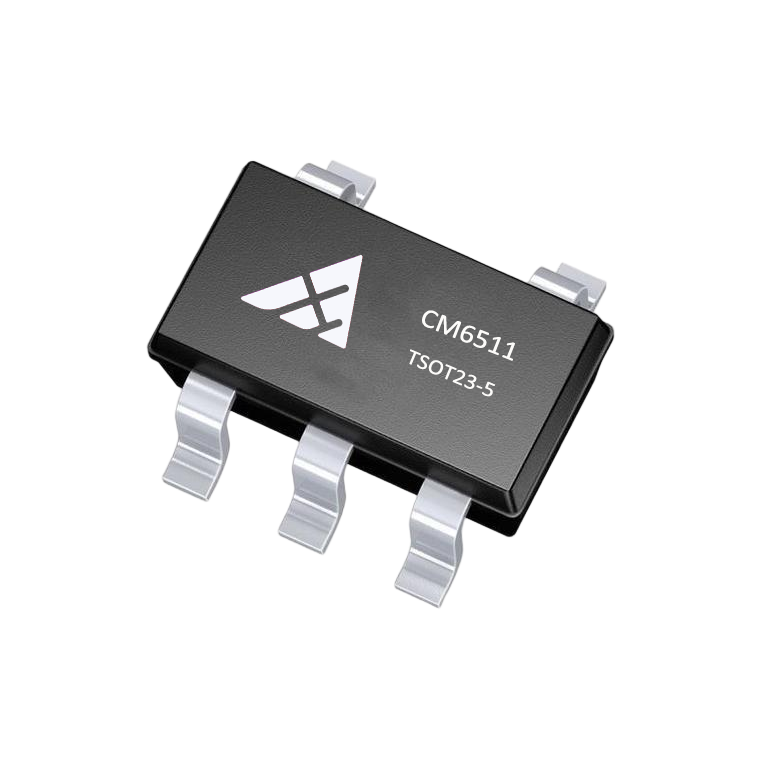
High-Performance MOSFET Die Chip Solutions - Advanced Power Management Technology

All Categories
Get a Quote

Get a Free Quote

Our representative will contact you soon.
Email
Name
Company Name
Message
0/1000

mosfet die chip

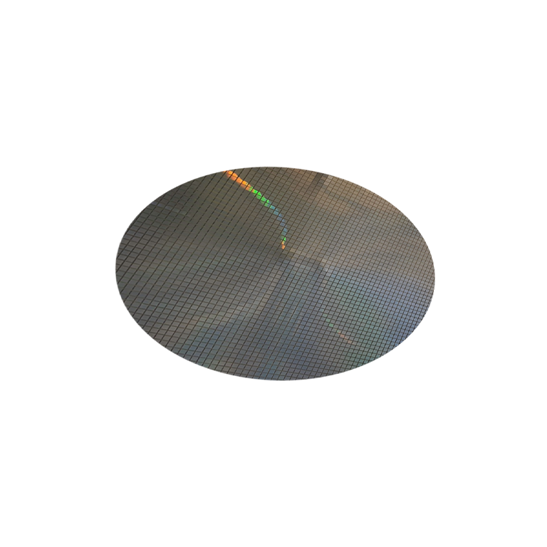
The mosfet die chip represents a fundamental breakthrough in semiconductor technology, serving as the core component that enables efficient power switching and amplification in countless electronic applications. As a bare semiconductor wafer containing the actual transistor elements, the mosfet die chip forms the heart of power management systems across industries. This microscopic yet powerful component consists of carefully engineered silicon layers that create the metal-oxide-semiconductor field-effect transistor structure, allowing precise control of electrical current flow through voltage application at the gate terminal. The mosfet die chip operates on the principle of field-effect modulation, where an electric field controls the conductivity of a semiconductor channel between source and drain terminals. This mechanism enables the chip to function as an electronic switch or variable resistor, making it indispensable for voltage regulation, motor control, and power conversion applications. Manufacturing processes for mosfet die chips involve advanced photolithography, ion implantation, and metallization techniques that create microscopic structures with incredible precision. The chip features multiple layers including the substrate, gate oxide, polysilicon gate, and metal interconnects, all working together to achieve optimal electrical performance. Temperature stability and thermal management capabilities are built into the mosfet die chip design, ensuring reliable operation across wide temperature ranges. The compact form factor of the mosfet die chip allows for high-density integration in space-constrained applications while maintaining excellent electrical characteristics. Advanced doping techniques and crystal structure optimization enable the mosfet die chip to handle high voltages and currents efficiently. Modern mosfet die chips incorporate features like low on-resistance, fast switching speeds, and reduced parasitic capacitance, making them essential for high-frequency applications and energy-efficient designs.

New Products

The mosfet die chip delivers exceptional energy efficiency that directly translates to reduced power consumption and lower operating costs for end users. This efficiency stems from the chip's ability to minimize power losses during switching operations, resulting in cooler operation and extended component lifespan. The superior thermal characteristics of the mosfet die chip eliminate the need for complex cooling systems in many applications, reducing overall system costs and maintenance requirements. Fast switching capabilities enable the mosfet die chip to respond instantly to control signals, providing precise power management and improved system responsiveness. This rapid switching performance makes the chip ideal for high-frequency applications where timing accuracy is critical. The mosfet die chip offers excellent voltage handling capacity, allowing designers to use fewer components in series while maintaining safety margins and system reliability. Compact size advantages of the mosfet die chip enable smaller product designs without compromising performance, helping manufacturers create more portable and space-efficient solutions. The chip's robust construction ensures long-term reliability even in harsh operating environments, reducing warranty costs and improving customer satisfaction. Low gate drive requirements of the mosfet die chip simplify control circuit design and reduce power consumption in the driving stage. This characteristic makes the chip particularly suitable for battery-powered applications where every milliwatt of power savings extends operating time. The mosfet die chip provides excellent linearity and low distortion characteristics, ensuring high-quality signal processing in audio and communication applications. Cost-effectiveness represents another significant advantage, as the mosfet die chip offers superior performance at competitive prices compared to alternative technologies. Manufacturing scalability allows for consistent quality and pricing across large production volumes. The chip's compatibility with standard mounting and connection methods simplifies integration into existing designs and manufacturing processes. Thermal stability ensures consistent performance across temperature variations, reducing the need for compensation circuits and improving overall system reliability. The mosfet die chip's high input impedance minimizes loading effects on control circuits, allowing for simpler and more efficient system designs.

Latest News

Is Your ADC/DAC Underperforming? The Culprit Could Be Your Voltage Reference

24

Nov

Is Your ADC/DAC Underperforming? The Culprit Could Be Your Voltage Reference

In the realm of precision analog-to-digital and digital-to-analog conversion, engineers often focus on the specifications of the ADC or DAC itself while overlooking a critical component that can make or break system performance. The voltage reference...
View More
Speed Meets Accuracy: Selecting High-Speed Data Converters for Demanding Applications

07

Jan

Speed Meets Accuracy: Selecting High-Speed Data Converters for Demanding Applications

In today's rapidly evolving industrial landscape, the demand for high-speed data converters has reached unprecedented levels. These critical components serve as the bridge between analog and digital domains, enabling sophisticated control systems to ...
View More
High-Performance ADC Chips and Precision DACs: Analysis of High-Speed, Low-Power Domestic Alternatives

02

Feb

High-Performance ADC Chips and Precision DACs: Analysis of High-Speed, Low-Power Domestic Alternatives

The semiconductor industry has witnessed unprecedented growth in demand for high-performance analog-to-digital converter chips and precision digital-to-analog converters. As electronic systems become increasingly sophisticated, the need for reliable,...
View More
High-Performance Instrumentation Amplifiers: Minimizing Noise in Low-Level Signal Gain

03

Feb

High-Performance Instrumentation Amplifiers: Minimizing Noise in Low-Level Signal Gain

Modern industrial applications demand exceptional precision when handling low-level signals, making instrumentation amplifiers a cornerstone technology in measurement and control systems. These specialized amplifiers provide high gain while maintaini...
View More

Get a Free Quote

Our representative will contact you soon.
Email
Name
Company Name
Message
0/1000

mosfet die chip

Superior Power Efficiency and Thermal Performance

Superior Power Efficiency and Thermal Performance

The mosfet die chip revolutionizes power management through its exceptional efficiency characteristics that significantly reduce energy waste and heat generation. This advanced semiconductor component achieves remarkably low on-resistance values, typically ranging from milliohms to a few ohms depending on the specific design requirements. The low resistance directly translates to minimal power dissipation during conduction, allowing the mosfet die chip to handle substantial currents while generating minimal heat. This thermal efficiency eliminates the need for elaborate cooling systems in many applications, reducing both initial costs and ongoing maintenance expenses. The chip's optimized silicon crystal structure and advanced doping techniques contribute to its superior electrical properties, enabling current flow with minimal resistance losses. Temperature coefficient characteristics of the mosfet die chip remain stable across wide operating ranges, ensuring consistent performance from arctic conditions to high-temperature industrial environments. The thermal design of the chip incorporates efficient heat spreading techniques that distribute thermal energy evenly across the die surface, preventing hot spots that could compromise reliability. Advanced packaging technologies compatible with the mosfet die chip further enhance thermal management through improved heat transfer to external heat sinks or PCB copper layers. The combination of low power losses and excellent thermal characteristics makes the mosfet die chip an ideal choice for energy-conscious applications including electric vehicles, renewable energy systems, and battery-powered devices. Users benefit from extended battery life, reduced cooling requirements, and lower electricity costs, making the mosfet die chip a financially attractive solution for long-term operations. The environmental impact is also significantly reduced due to lower energy consumption and reduced waste heat generation.
Ultra-Fast Switching Speed and Control Precision

Ultra-Fast Switching Speed and Control Precision

The mosfet die chip excels in high-speed switching applications through its exceptionally fast response characteristics and precise control capabilities. Advanced gate structure design minimizes parasitic capacitances that typically slow switching transitions, enabling the chip to turn on and off within nanoseconds. This rapid switching ability makes the mosfet die chip indispensable for high-frequency power conversion applications including switch-mode power supplies, motor drives, and RF amplification systems. The precise control offered by the mosfet die chip stems from its voltage-controlled operation, where small gate voltage changes produce predictable and linear responses in drain current. This characteristic enables sophisticated control algorithms and feedback systems that optimize performance in real-time applications. Low gate charge requirements mean that the mosfet die chip can be driven efficiently by low-power control circuits, reducing overall system complexity and power consumption. The chip's excellent switching characteristics minimize electromagnetic interference and switching losses, contributing to cleaner operation and improved efficiency in sensitive electronic environments. Fast switching speeds enable higher operating frequencies, allowing designers to use smaller passive components such as inductors and capacitors, resulting in more compact and cost-effective designs. The mosfet die chip maintains consistent switching characteristics across temperature variations and aging, ensuring reliable long-term performance without drift or degradation. Advanced fabrication processes create uniform electrical characteristics across the entire die surface, eliminating performance variations that could affect switching precision. These fast switching capabilities make the mosfet die chip particularly valuable in applications requiring precise timing control, such as synchronous rectification, Class-D audio amplifiers, and high-resolution motor control systems. The combination of speed and precision enables more sophisticated control strategies that improve overall system performance and user experience.
Exceptional Reliability and Durability Standards

Exceptional Reliability and Durability Standards

The mosfet die chip demonstrates outstanding reliability characteristics that ensure consistent performance throughout extended operational lifespans, making it a dependable choice for critical applications. Advanced semiconductor processing techniques create uniform crystal structures within the chip that resist degradation from electrical stress, temperature cycling, and environmental factors. The robust gate oxide layer in the mosfet die chip provides excellent isolation and prevents leakage currents that could compromise performance or cause premature failure. Comprehensive testing protocols during manufacturing ensure that each mosfet die chip meets strict quality standards before shipment, reducing field failure rates and improving customer satisfaction. The chip's design incorporates built-in protection features including avalanche energy handling capability and thermal shutdown mechanisms that prevent damage from overcurrent or overtemperature conditions. These protective features allow the mosfet die chip to survive fault conditions that would destroy other semiconductor devices, reducing system downtime and repair costs. Advanced metallization systems used in the mosfet die chip resist electromigration and corrosion, maintaining reliable electrical connections throughout the device lifetime. The silicon substrate and junction designs are optimized to handle repetitive switching stress without degradation, enabling millions of switching cycles without performance loss. Extensive qualification testing including temperature cycling, humidity exposure, and electrical stress screening validates the long-term reliability of the mosfet die chip under real-world operating conditions. The chip's stable electrical characteristics over time eliminate the need for frequent recalibration or adjustment, reducing maintenance requirements and operational costs. Proven track records in demanding applications such as automotive electronics, industrial automation, and aerospace systems demonstrate the exceptional reliability that customers can expect from the mosfet die chip. Quality manufacturing processes and materials ensure consistent performance across production lots, providing predictable behavior for design engineers and system integrators.

Get a Free Quote

Our representative will contact you soon.
Email
Name
Company Name
Message
0/1000