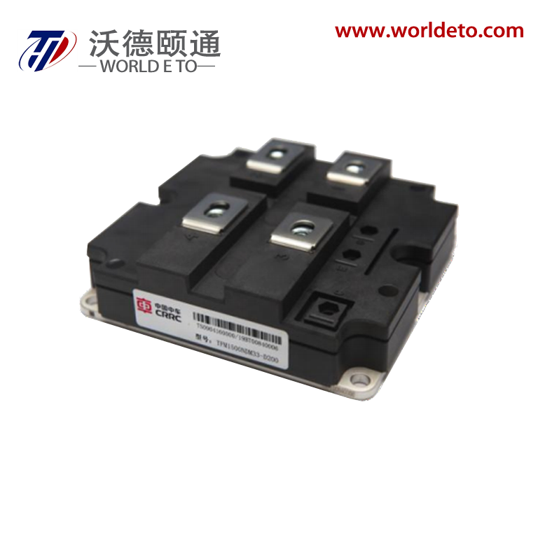
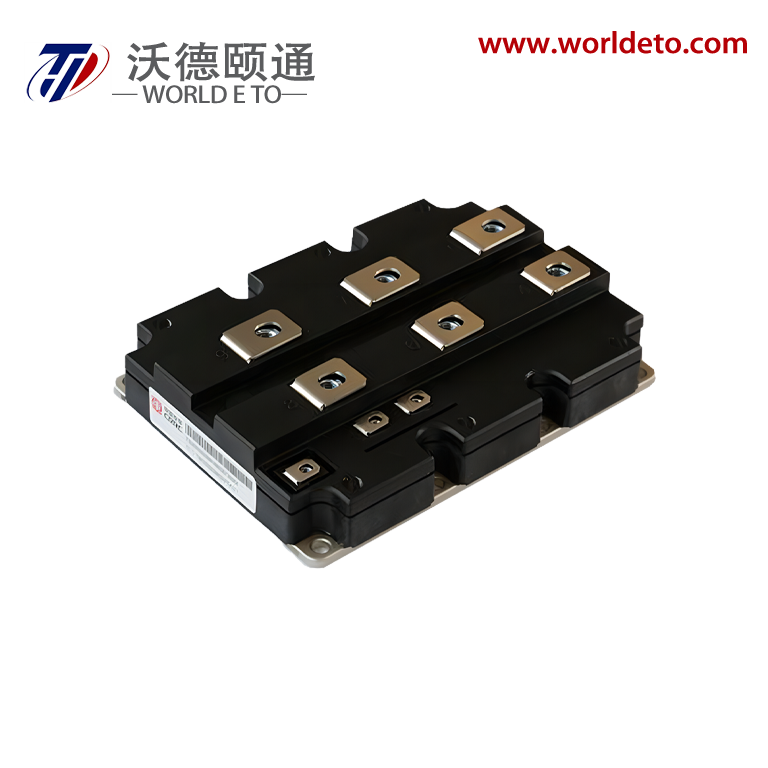
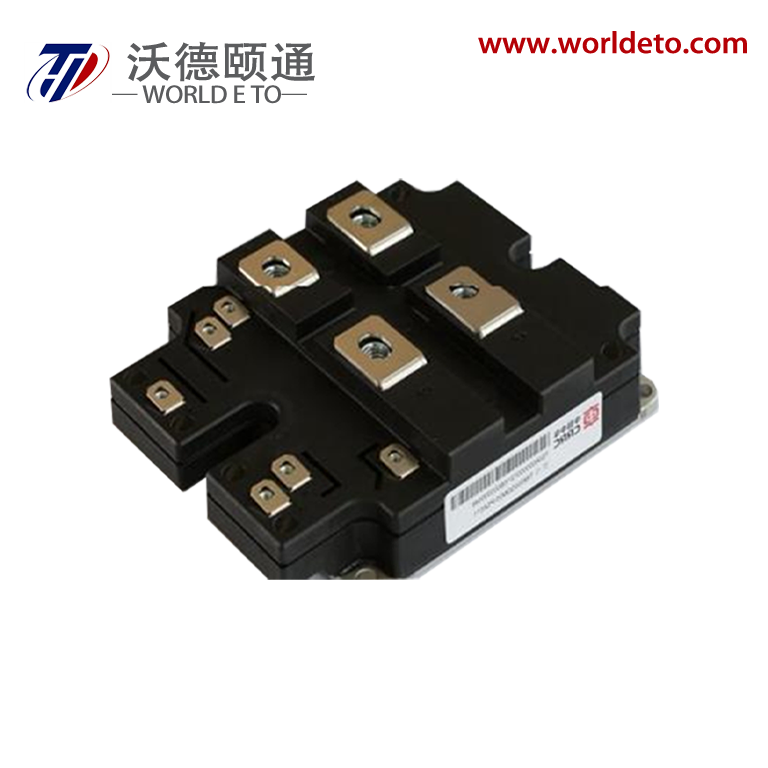
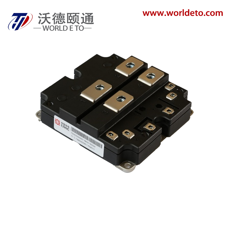
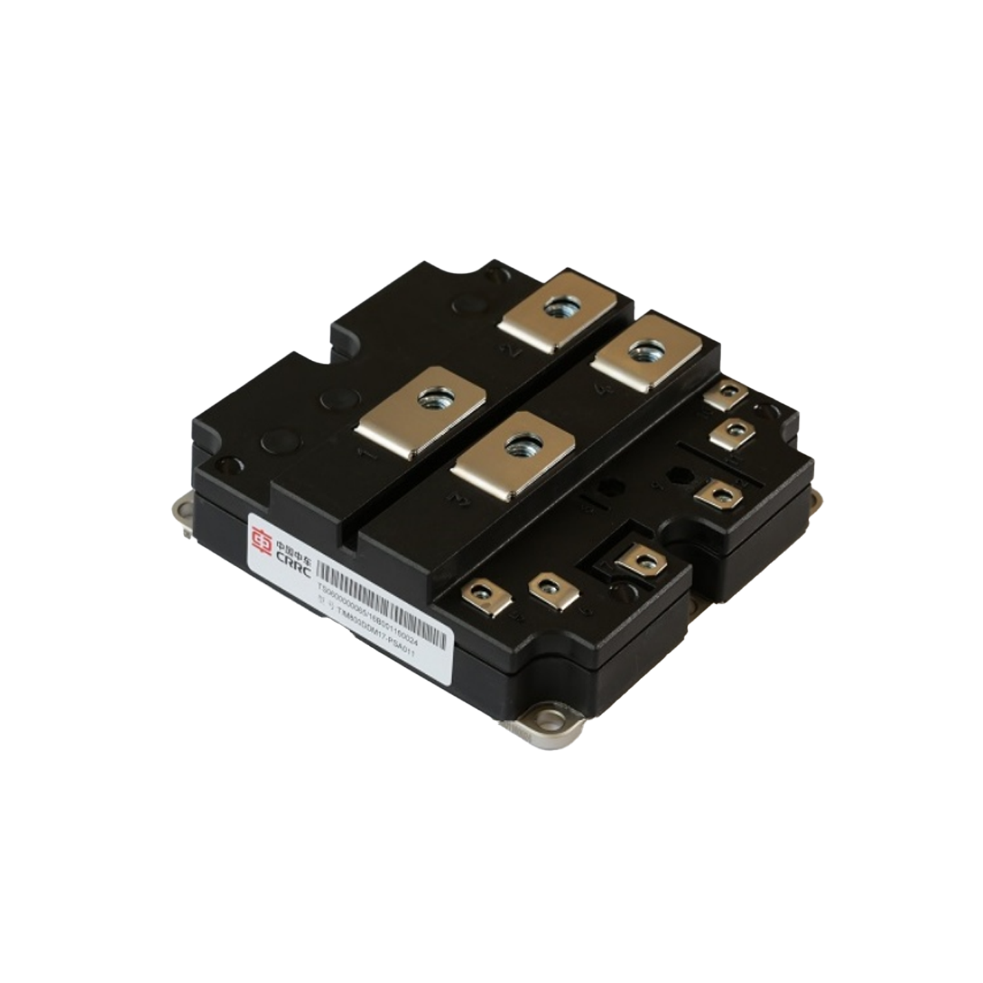
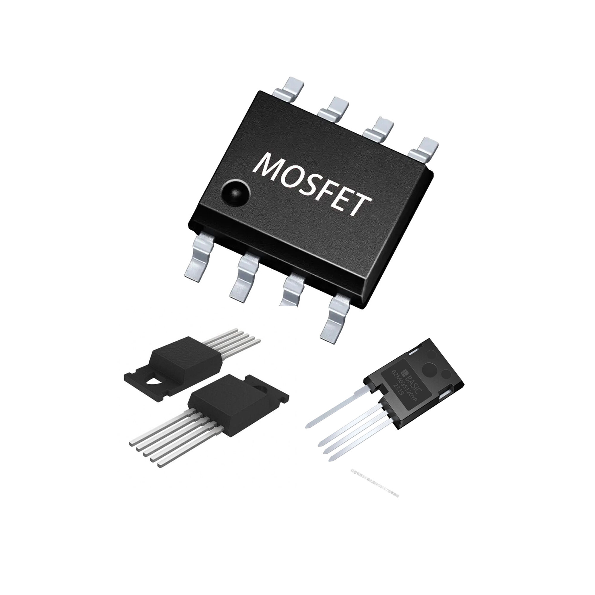
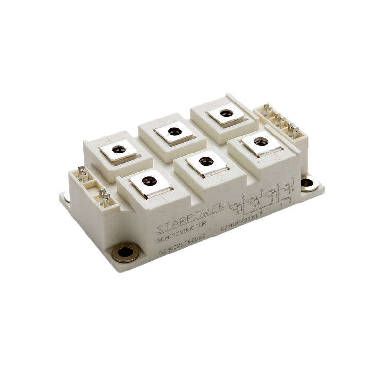
MOSFET Discrete Die: Advanced Power Switching Solutions for High-Efficiency Electronics

All Categories
Get a Quote

Get a Free Quote

Our representative will contact you soon.
Email
Name
Company Name
Message
0/1000

mosfet discrete die

The mosfet discrete die represents a fundamental breakthrough in semiconductor technology, offering engineers and manufacturers unprecedented control over power management and switching applications. This compact, single-chip solution delivers exceptional performance characteristics that make it indispensable across numerous electronic systems. The mosfet discrete die operates as a voltage-controlled switch, utilizing metal-oxide-semiconductor field-effect transistor technology to regulate electrical current flow with remarkable precision and efficiency. Its primary functions include power amplification, signal switching, and voltage regulation, making it essential for modern electronic devices ranging from smartphones to industrial machinery. The technological architecture of the mosfet discrete die incorporates advanced silicon processing techniques that enable superior thermal management and electrical isolation. This design methodology ensures optimal performance under varying operating conditions while maintaining structural integrity throughout extended operational cycles. The mosfet discrete die features three critical terminals: gate, source, and drain, which work together to control current flow based on applied gate voltage. This configuration allows for precise switching operations with minimal power loss, contributing significantly to overall system efficiency. Manufacturing processes for mosfet discrete die involve sophisticated fabrication techniques that create highly pure silicon substrates with precisely controlled doping profiles. These processes result in devices with excellent electrical characteristics, including low on-resistance, fast switching speeds, and high breakdown voltages. Applications for mosfet discrete die span across automotive electronics, consumer appliances, telecommunications infrastructure, renewable energy systems, and industrial automation equipment. The versatility of the mosfet discrete die makes it particularly valuable in power conversion circuits, motor control systems, and battery management applications where efficiency and reliability are paramount. Modern mosfet discrete die implementations incorporate advanced packaging technologies that enhance thermal dissipation and electrical performance while reducing overall footprint requirements.

Popular Products

The mosfet discrete die delivers substantial benefits that directly impact system performance and operational costs for manufacturers and end-users alike. Superior efficiency stands as the primary advantage, with modern mosfet discrete die achieving switching efficiencies exceeding 95 percent in many applications. This exceptional efficiency translates to reduced energy consumption, lower operating temperatures, and extended battery life in portable devices. The high switching speed capability of mosfet discrete die enables faster response times in control circuits, improving overall system responsiveness and performance quality. Cost-effectiveness emerges as another significant benefit, as mosfet discrete die solutions often require fewer external components compared to alternative switching technologies, reducing bill-of-materials costs and simplifying circuit design complexity. The compact form factor of mosfet discrete die allows engineers to create smaller, lighter products while maintaining or improving performance specifications. This miniaturization capability proves particularly valuable in space-constrained applications such as mobile electronics and automotive systems. Thermal management advantages of mosfet discrete die include lower heat generation during operation, which reduces cooling requirements and improves system reliability. The reduced thermal stress extends component lifespan and minimizes maintenance needs, providing long-term cost savings for manufacturers and users. Voltage handling capabilities of mosfet discrete die cover a wide range, from low-voltage logic applications to high-voltage power systems, offering design flexibility across diverse projects. The fast switching characteristics of mosfet discrete die minimize switching losses and electromagnetic interference, contributing to cleaner power delivery and better electromagnetic compatibility in sensitive applications. Design flexibility represents another key advantage, as mosfet discrete die can be configured for various topologies including buck converters, boost converters, and bridge circuits. This adaptability allows engineers to optimize designs for specific performance requirements without compromising efficiency or reliability. Manufacturing scalability of mosfet discrete die production enables cost-effective volume manufacturing while maintaining consistent quality standards. The mature manufacturing processes ensure reliable supply chains and predictable pricing structures for long-term projects. Environmental benefits include reduced power consumption leading to lower carbon footprints and compliance with energy efficiency regulations across global markets.

Practical Tips

Selecting the Right High-Performance In-Amp for Precision Measurement Systems

24

Nov

Selecting the Right High-Performance In-Amp for Precision Measurement Systems

Precision measurement systems form the backbone of modern industrial applications, from aerospace instrumentation to medical device calibration. At the heart of these systems lies a critical component that determines measurement accuracy and signal i...
View More
Low-Power Design Secrets: Utilizing Precision LDOs and Voltage References for Extended Battery Life

07

Jan

Low-Power Design Secrets: Utilizing Precision LDOs and Voltage References for Extended Battery Life

Modern electronic systems demand increasingly sophisticated power management strategies to achieve extended battery life while maintaining optimal performance. The integration of precision LDOs and voltage references has become a cornerstone of effic...
View More
Building Reliable Systems: The Role of Precision Voltage References and LDOs in Industrial Applications

07

Jan

Building Reliable Systems: The Role of Precision Voltage References and LDOs in Industrial Applications

Industrial automation and control systems demand unwavering accuracy and reliability to ensure optimal performance across diverse operating conditions. At the heart of these sophisticated systems lie critical components that provide stable power mana...
View More
Breaking Speed Barriers: The Future of High-Speed ADCs in Modern Communication

03

Feb

Breaking Speed Barriers: The Future of High-Speed ADCs in Modern Communication

The telecommunications industry continues to push the boundaries of data transmission speeds, driving unprecedented demand for advanced analog-to-digital conversion technologies. High-speed ADCs have emerged as the cornerstone of modern communication...
View More

Get a Free Quote

Our representative will contact you soon.
Email
Name
Company Name
Message
0/1000

mosfet discrete die

Ultra-Low On-Resistance Technology

Ultra-Low On-Resistance Technology

The mosfet discrete die incorporates cutting-edge ultra-low on-resistance technology that fundamentally transforms power efficiency in electronic systems. This advanced characteristic represents a crucial performance metric that directly impacts overall system efficiency, thermal management, and operational reliability. When a mosfet discrete die operates in its fully conducting state, the on-resistance determines how much power is dissipated as heat rather than delivered to the load. Modern mosfet discrete die designs achieve remarkably low on-resistance values, often measured in milliohms, which translates to minimal conduction losses during normal operation. This technological advancement stems from sophisticated semiconductor processing techniques that optimize the channel structure and minimize parasitic resistances throughout the device. The ultra-low on-resistance capability of mosfet discrete die enables designers to achieve higher power densities while maintaining acceptable thermal profiles, allowing for more compact and efficient system designs. In practical applications, this translates to longer battery life in portable devices, reduced cooling requirements in power supplies, and improved overall system reliability. The economic impact of ultra-low on-resistance technology extends beyond initial efficiency gains, as reduced heat generation minimizes the need for extensive thermal management solutions, including heat sinks, fans, and thermal interface materials. This reduction in auxiliary components leads to lower system costs, reduced weight, and improved reliability through fewer potential failure points. Manufacturing processes for achieving ultra-low on-resistance in mosfet discrete die involve precise control of dopant concentrations, gate oxide thickness, and channel geometry. These parameters are optimized through advanced simulation tools and experimental validation to ensure consistent performance across production volumes. The temperature coefficient of on-resistance in modern mosfet discrete die designs has been engineered to minimize performance degradation over operating temperature ranges, ensuring stable efficiency throughout various environmental conditions. Quality control measures for ultra-low on-resistance mosfet discrete die include comprehensive electrical testing at multiple temperature points and statistical process control methods that maintain tight parameter distributions across manufacturing lots.
Advanced Thermal Management Integration

Advanced Thermal Management Integration

The mosfet discrete die incorporates sophisticated thermal management integration that addresses one of the most critical challenges in modern electronic design: effective heat dissipation. This advanced thermal architecture enables reliable operation under demanding conditions while maintaining optimal performance characteristics throughout extended operational periods. The thermal management integration within mosfet discrete die begins at the silicon level, where careful attention to chip layout and metallization patterns optimizes heat flow paths from active regions to packaging interfaces. This foundational approach ensures efficient thermal conduction while minimizing hot spot formation that could compromise device reliability. The package design of mosfet discrete die incorporates advanced thermal interface materials and optimized lead frame configurations that facilitate superior heat transfer to external thermal management systems. These design elements work together to create thermal resistance values that enable higher power handling capabilities within compact form factors. Thermal modeling and simulation play crucial roles in optimizing the thermal management integration of mosfet discrete die, allowing engineers to predict temperature distributions under various operating conditions and optimize designs accordingly. Advanced computational fluid dynamics analysis ensures that thermal management integration meets stringent reliability requirements while maximizing performance potential. The junction-to-case thermal resistance of modern mosfet discrete die represents significant improvements over previous generations, enabling higher current handling capabilities and improved thermal cycling resistance. This enhancement directly translates to longer device lifespans and reduced failure rates in demanding applications. Thermal management integration also encompasses considerations for thermal cycling resistance, ensuring that mosfet discrete die can withstand repeated temperature excursions without degradation in electrical performance or mechanical integrity. This capability proves essential in automotive and industrial applications where temperature variations are routine. Package innovations for thermal management integration include exposed pad designs, thermal vias, and optimized copper areas that enhance heat spreading and transfer efficiency. These features enable system designers to achieve better thermal performance with standard PCB technologies and conventional cooling methods. The testing and validation of thermal management integration involve comprehensive thermal characterization under various operating conditions, ensuring that mosfet discrete die meets specified thermal performance requirements across production volumes and operating environments.
High-Speed Switching Performance

High-Speed Switching Performance

The mosfet discrete die delivers exceptional high-speed switching performance that enables precise control and efficient operation in demanding applications requiring rapid state transitions. This advanced switching capability represents a cornerstone feature that distinguishes modern mosfet discrete die from conventional switching technologies, offering significant advantages in terms of efficiency, electromagnetic compatibility, and system responsiveness. The high-speed switching performance of mosfet discrete die stems from optimized gate structure designs that minimize parasitic capacitances while maintaining robust gate oxide integrity. These design optimizations result in faster charging and discharging of gate capacitance, enabling rapid transitions between conducting and non-conducting states. The switching speed characteristics directly impact power loss reduction, as faster transitions minimize the time spent in the linear region where simultaneous voltage and current presence causes power dissipation. Advanced processing techniques used in manufacturing mosfet discrete die contribute significantly to high-speed switching performance through precise control of channel mobility and threshold voltage characteristics. These parameters are carefully optimized to ensure consistent switching behavior across temperature and voltage variations while maintaining long-term reliability. The gate drive requirements for achieving optimal high-speed switching performance in mosfet discrete die are engineered to be compatible with standard driver circuits, eliminating the need for specialized or complex driving circuitry in most applications. This compatibility ensures ease of implementation while maintaining superior switching performance characteristics. Electromagnetic interference considerations for high-speed switching mosfet discrete die include careful attention to package inductances and capacitances that could affect switching waveforms and generate unwanted emissions. Modern designs incorporate features that minimize these parasitic elements while maintaining mechanical robustness and thermal performance. The measurement and characterization of high-speed switching performance in mosfet discrete die involve sophisticated test equipment capable of accurately capturing fast transition times and associated parameters such as rise time, fall time, and switching losses. These measurements ensure that devices meet specified performance criteria and enable proper application optimization. System-level benefits of high-speed switching performance include improved power conversion efficiency, reduced filtering requirements, and enhanced dynamic response in control applications. These advantages translate to more compact designs, lower costs, and improved overall system performance. Quality assurance for high-speed switching performance encompasses comprehensive testing across temperature ranges, supply voltages, and load conditions to ensure consistent behavior in real-world applications.

Get a Free Quote

Our representative will contact you soon.
Email
Name
Company Name
Message
0/1000