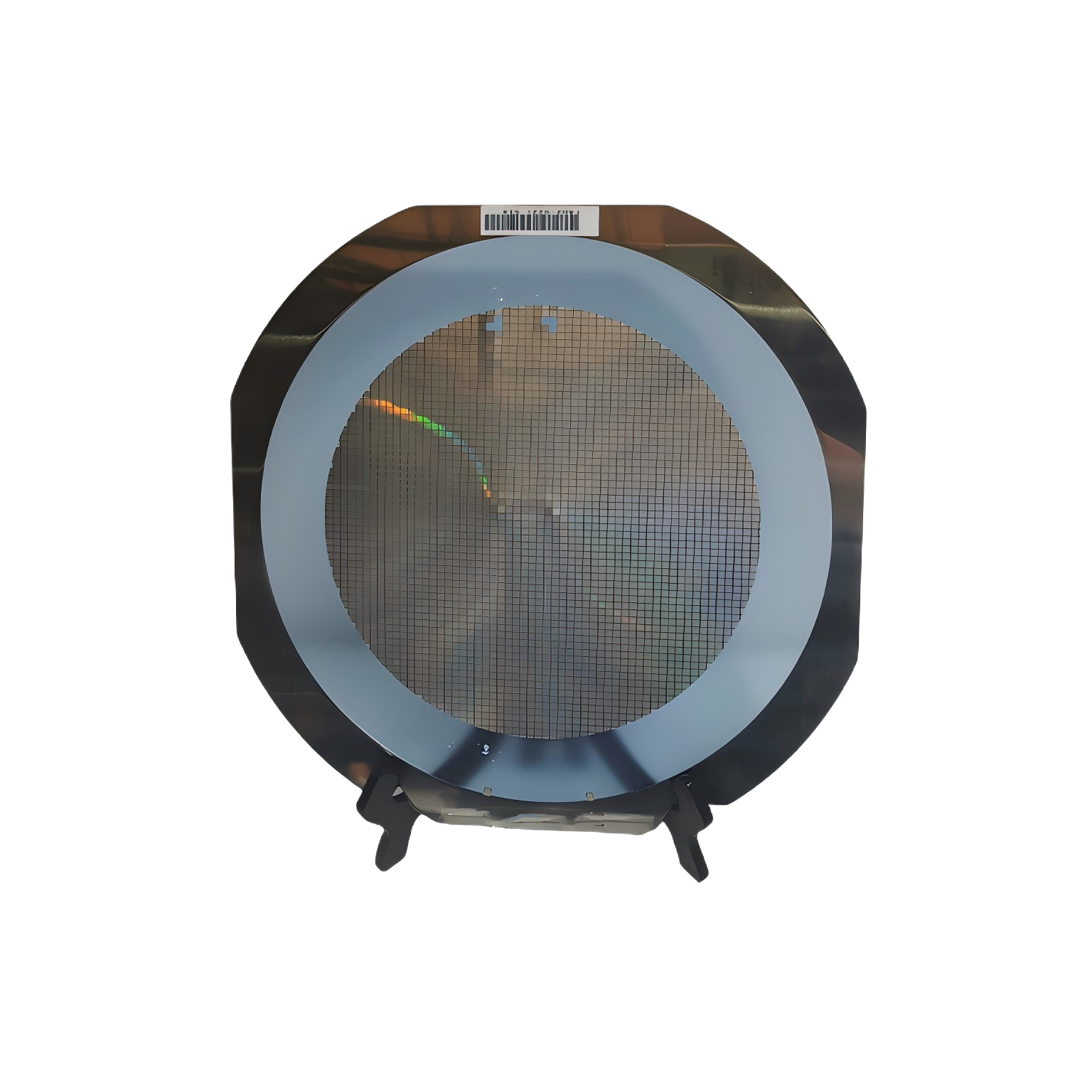
In modern power electronics, switching losses represent one of the most persistent challenges facing circuit designers, inverter engineers, and power module developers. At the heart of this challenge lies a phenomenon known as reverse recovery charge, a transient burst of charge that flows in the wrong direction during diode turn-off and generates heat, electromagnetic interference, and efficiency losses. The FRD wafer — the semiconductor substrate at the core of fast recovery diodes — has become the primary battleground where engineers are fighting to minimize this destructive charge and unlock higher system efficiency.
Advanced FRD wafer technology is no longer just an incremental refinement. It represents a fundamental shift in how minority carrier dynamics, epitaxial layer architecture, and lifetime control techniques are engineered at the wafer level to suppress reverse recovery charge. For engineers designing high-frequency converters, motor drives, EV charging systems, and industrial inverters, understanding what drives these wafer-level improvements — and how they translate into measurable circuit performance gains — is essential knowledge for making sound component and design decisions.
The Physics Behind Reverse Recovery Charge in Fast Recovery Diodes
What Reverse Recovery Charge Actually Represents
Reverse recovery charge, denoted as Qrr, is the amount of charge that must be extracted from a diode before it can block reverse voltage. When a fast recovery diode conducts forward current and is then switched off, the minority carriers stored in the junction do not disappear instantly. They must recombine or be swept out of the depletion region, and during this process, a reverse current pulse flows through the circuit — a pulse that carries real energy, generates real heat, and stresses both the diode and the associated switching transistor.
The magnitude of Qrr is directly tied to the volume and distribution of stored minority carriers in the FRD wafer's epitaxial layer. A thicker or more heavily injected base region will store more carriers, producing a larger Qrr and a longer recovery time. Engineers working on power systems quickly learn that Qrr is not just a specification number — it is a dynamic quantity influenced by forward current, junction temperature, and the rate of current commutation (di/dt). Advanced FRD wafer designs must account for all these variables simultaneously.
The consequences of high Qrr cascade through an entire circuit. The reverse recovery current spike creates voltage overshoot across circuit inductances, forcing designers to add snubber networks or derate switching speeds. Electromagnetic interference (EMI) from the sharp current transient requires additional filtering. Thermal management becomes more demanding as recovery losses accumulate, particularly in applications operating at switching frequencies above 10 kHz. Reducing Qrr at the FRD wafer level is therefore one of the highest-leverage improvements available to power circuit designers.
How Carrier Lifetime Governs Qrr at the Wafer Level
Within the FRD wafer, minority carrier lifetime is the single most influential physical parameter controlling reverse recovery behavior. A shorter carrier lifetime means stored carriers recombine faster, reducing the charge available for reverse recovery. However, shortening carrier lifetime also increases forward voltage drop because it limits conductivity modulation — the mechanism that allows a thin, lightly doped base to carry high current without excessive resistive losses. This fundamental tension between Qrr reduction and forward voltage penalty defines the core design challenge at the FRD wafer level.
Traditional lifetime control techniques relied on gold diffusion or electron irradiation applied uniformly to the entire FRD wafer. While effective at reducing minority carrier lifetime, these methods tend to produce abrupt, 'snappy' recovery behavior where the reverse current drops sharply, generating voltage spikes that can damage circuit components. Advanced wafer processing techniques have moved toward spatially controlled, graded lifetime profiles that produce softer recovery — a more gradual decay of reverse current that reduces peak voltage overshoot without sacrificing the Qrr reduction benefit.
Advanced FRD Wafer Architectures That Minimize Reverse Recovery Charge
Controlled Epitaxial Layer Design for Optimized Carrier Distribution
The epitaxial layer grown on the FRD wafer substrate is the primary active region where carrier dynamics play out. Advanced epitaxial design controls the doping profile, thickness, and resistivity of this layer with precision to minimize the volume of stored charge while maintaining adequate breakdown voltage and forward current capability. Thinner epitaxial layers with carefully graded doping profiles can achieve lower Qrr without proportionally increasing forward voltage, because the reduction in stored charge outweighs the modest increase in resistive drop.
Modern FRD wafer manufacturing uses metal-organic chemical vapor deposition (MOCVD) or similar advanced growth techniques to achieve epitaxial layer thickness uniformity within a few percent across the wafer surface. This uniformity is critical because variations in epilayer thickness translate directly into variations in Qrr and forward voltage across a production lot. Tight epitaxial control enables more consistent performance and reduces the need for over-design margins that would otherwise inflate component costs or degrade efficiency.
The interface between the epitaxial layer and the substrate in an FRD wafer also plays a role in recovery behavior. Abrupt interfaces can introduce recombination centers that are difficult to control, while graded transitions allow more predictable minority carrier behavior. Advanced wafer suppliers invest significant process development effort into optimizing these interfaces, recognizing that Qrr performance in the final diode is often limited by interface quality as much as by bulk epitaxial properties.
Proton Irradiation and Local Lifetime Control Techniques
One of the most significant advances in FRD wafer processing is the use of proton irradiation to introduce recombination centers at precisely controlled depths within the wafer. Unlike electron irradiation, which distributes damage relatively uniformly, proton irradiation deposits its peak damage at a depth that depends on the beam energy. By tuning the proton energy, process engineers can position the highest recombination center density exactly where stored minority carriers are most concentrated during forward conduction — typically near the anode-side of the drift region in a fast recovery diode.
This localized lifetime control approach in the FRD wafer architecture allows a dramatic reduction in Qrr while preserving carrier lifetime in the regions that contribute most to conductivity modulation and forward voltage performance. The result is a diode with what engineers describe as a 'soft' recovery characteristic — the reverse current decays gradually rather than snapping off, minimizing the voltage spike across circuit inductances. Proton irradiation has become a standard technique among advanced FRD wafer producers precisely because it addresses the snappiness problem that plagued earlier lifetime-control approaches.
After irradiation, the FRD wafer undergoes a controlled anneal that partially recovers the crystal lattice while leaving the desired recombination centers intact. The anneal conditions — temperature, duration, and atmosphere — must be carefully optimized for each wafer design. Too little annealing leaves excess recombination damage that increases leakage current; too much annealing removes the recombination centers that are needed to suppress Qrr. This process sensitivity is one reason why advanced FRD wafer technology requires significant manufacturing expertise to execute reliably.
Field-Stop and Buffer Layer Integration in FRD Wafer Design
Field-stop layer technology, originally developed for IGBTs, has found important application in advanced FRD wafer design. A field-stop layer is a moderately doped n-type region placed between the lightly doped drift region and the heavily doped cathode substrate. When the diode is blocking reverse voltage, the depletion region expands through the drift layer until it encounters the field-stop layer, which abruptly terminates the electric field. This allows the use of a thinner drift region for a given breakdown voltage specification, directly reducing the volume of stored minority carriers and therefore the potential Qrr.
In an FRD wafer incorporating a field-stop architecture, the device can be designed with a significantly thinner active layer than would be required in a punch-through or non-punch-through structure. The thinner layer means fewer minority carriers must be swept out or recombined during turn-off, leading to lower Qrr at equivalent forward voltage performance. Field-stop FRD wafer designs are particularly well-suited to applications in the 600V to 1700V blocking voltage range, where the trade-off between drift layer thickness and on-state losses is most acute.
Temperature Dependence of Qrr and Its Implications for FRD Wafer Selection
How Junction Temperature Amplifies Reverse Recovery Charge
A critical but often underappreciated aspect of reverse recovery behavior is its strong dependence on junction temperature. As the junction temperature of a fast recovery diode increases, minority carrier lifetime in the FRD wafer typically increases as well, because phonon scattering and other thermally activated recombination mechanisms become less effective at elevated temperatures. The result is that Qrr can increase by a factor of two to four between room temperature and maximum rated junction temperature, even in diodes that appear well-optimized at 25°C.
This temperature sensitivity has direct implications for system-level design. An FRD wafer architecture optimized for low Qrr at room temperature may still produce unacceptable recovery losses in a high-temperature operating environment. Engineers evaluating FRD wafer products must examine Qrr at the actual junction temperatures their application will sustain, not just at the standard 25°C datasheet condition. Advanced wafer designs that incorporate temperature-stable lifetime control mechanisms — such as certain types of deep-level recombination centers introduced by proton irradiation — show flatter Qrr-versus-temperature curves, making them better suited to thermally demanding applications.
Designing for Worst-Case Thermal and Switching Conditions
The interaction between di/dt, junction temperature, and FRD wafer architecture determines the worst-case reverse recovery stress in a real circuit. Higher di/dt during commutation sweeps carriers out of the junction more rapidly, reducing the total Qrr but increasing the peak reverse recovery current (Irrm). The relationship between Qrr, Irrm, and the recovery softness factor depends on the internal carrier distribution profile in the FRD wafer, which in turn is shaped by epitaxial design and lifetime control techniques.
Advanced FRD wafer designs address worst-case conditions by engineering a recovery characteristic that degrades gracefully rather than catastrophically as temperature and switching speed increase. A diode with a soft recovery profile will maintain controlled, predictable behavior even when operating conditions deviate from nominal. This robustness is particularly valuable in motor drive and inverter applications where load transients can momentarily push diodes into extreme operating conditions that a snappy device would not survive without circuit protection measures.
System-Level Benefits of Advanced FRD Wafer Technology
Efficiency Gains in High-Frequency Power Conversion
The system-level impact of reduced Qrr from advanced FRD wafer technology becomes most apparent at higher switching frequencies. In a typical boost converter or active power factor correction (PFC) stage operating at 65 kHz, the recovery loss contribution from the freewheeling diode can represent 20 to 40 percent of total switching losses. Halving the Qrr through improved FRD wafer design therefore translates directly into a meaningful efficiency improvement at the system level — a gain that accumulates continuously over the operational life of the equipment.
For electric vehicle charging infrastructure, solar inverters, and industrial variable-frequency drives, these efficiency improvements have real economic value. A 1 to 2 percentage point gain in converter efficiency reduces operating costs, reduces cooling system requirements, and allows higher power density in the same thermal envelope. Engineers specifying the FRD wafer platform for these applications are therefore making a decision with compounding financial implications, not merely an incremental component substitution.
EMI Reduction and Reliability Improvements
Beyond efficiency, advanced FRD wafer technology delivers tangible benefits in EMI performance and long-term reliability. The voltage spike generated during reverse recovery is a primary source of conducted and radiated EMI in switching power supplies and motor drives. By reducing both the magnitude and the slope of the reverse current transient through improved FRD wafer design, the amplitude of these voltage spikes is reduced, easing EMI filter requirements and often allowing the elimination of snubber networks that would otherwise add cost, size, and losses to the circuit.
Reliability benefits flow from the reduced electrical stress that lower Qrr imposes on the associated switching transistors and gate drive circuits. Every reverse recovery event stresses the transistor that is turning on during commutation, because the reverse recovery current from the diode is added to the load current that the transistor must carry. A lower Qrr from the FRD wafer means lower peak current stress on the transistor, reduced power dissipation in gate resistors, and lower likelihood of parasitic turn-on events that can lead to shoot-through failures in half-bridge configurations.
FAQ
What is reverse recovery charge and why does it matter for FRD wafer selection?
Reverse recovery charge (Qrr) is the total charge that flows in the reverse direction through a diode during its turn-off transition. It originates from minority carriers stored in the FRD wafer's epitaxial region during forward conduction. High Qrr increases switching losses, generates EMI, and stresses companion transistors. Selecting an FRD wafer with low, temperature-stable Qrr is therefore critical for efficient, reliable power conversion.
How does proton irradiation reduce Qrr in an FRD wafer?
Proton irradiation introduces recombination centers at a precisely controlled depth within the FRD wafer by adjusting beam energy. These localized defects accelerate minority carrier recombination in the region where stored charge is highest, reducing Qrr without uniformly degrading carrier lifetime throughout the device. This technique produces softer recovery behavior compared to uniform irradiation methods, reducing voltage overshoot and improving circuit reliability.
Does junction temperature significantly affect the Qrr of an FRD wafer?
Yes, junction temperature has a strong effect on Qrr. As temperature rises, minority carrier lifetime in the FRD wafer typically increases, allowing more charge to accumulate during forward conduction. This causes Qrr to increase — sometimes by a factor of two to four between 25°C and maximum rated temperature. Engineers must evaluate FRD wafer performance at actual operating temperatures, not just at standard test conditions, to ensure adequate circuit performance under real-world conditions.
What applications benefit most from advanced FRD wafer technology with reduced Qrr?
Applications operating at high switching frequencies and elevated power levels gain the most from advanced FRD wafer technology. These include electric vehicle onboard chargers and DC fast chargers, solar inverters, industrial variable-frequency motor drives, active power factor correction stages, and server power supplies. In all these applications, switching losses dominate total power dissipation, and reducing Qrr through improved FRD wafer design directly improves efficiency, lowers thermal management costs, and reduces EMI filter complexity.