
 EN
EN
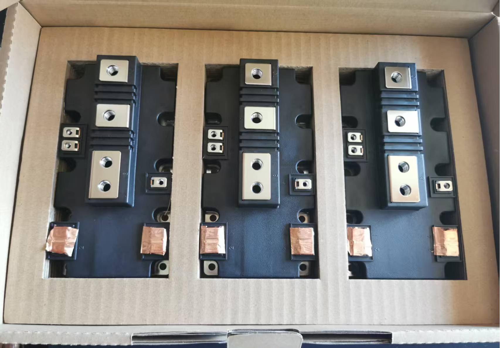
In high-power power electronics, the IGBT module plays a central role in controlling large currents and high voltages with precision. As switching frequencies increase and power densities grow, even small amounts of stray inductance within the IGBT module circuit layout can trigger dangerous voltage spikes, increase switching losses, and compromise the long-term reliability of the entire system. Engineers working with high-power IGBT module designs must treat stray inductance not as an acceptable side effect but as a critical parameter that demands deliberate engineering control.
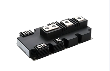
Stray inductance, often called parasitic inductance, arises from every conductive element in the power loop — including busbars, PCB traces, bond wires, and internal connections inside the IGBT module itself. When an IGBT module switches off rapidly, the energy stored in these inductive elements generates overvoltage transients. Without proper mitigation, these transients can exceed the rated voltage of the IGBT module and lead to catastrophic failure. This article explains how to identify, understand, and minimize stray inductance in high-power IGBT module designs through systematic layout, packaging, and circuit strategies.
Sources of Stray Inductance in an IGBT Module System
Internal Inductance Within the IGBT Module Package
Every IGBT module contains internal stray inductance that originates from bond wires, the substrate traces, and the module terminals. The bond wires connecting the silicon die to the copper substrate in an IGBT module are particularly inductive due to their length and loop geometry. Modern high-power IGBT module designs address this by replacing bond wires with sintered copper clips or press-pack structures that significantly reduce internal parasitic inductance. When selecting an IGBT module, it is important to review the datasheet for specified internal stray inductance values, as these directly affect the maximum allowable di/dt during switching events.
The substrate material and internal conductor routing within the IGBT module also contribute to inductance. Direct bonded copper substrates are preferred in high-power IGBT module designs because they offer low thermal resistance combined with compact conductor paths. Minimizing the internal loop area formed by the current path inside the IGBT module is a fundamental step toward reducing parasitic inductance at the source.
External Power Loop Inductance Surrounding the IGBT Module
Beyond the IGBT module itself, the external busbar and capacitor placement heavily influence the total stray inductance of the power loop. The current path from the DC bus capacitors through the busbars to the IGBT module terminals and back forms a loop whose area is directly proportional to the stray inductance generated. Even a well-designed IGBT module cannot compensate for a poorly routed external circuit. Engineers must ensure that the DC link capacitors are positioned as close as possible to the IGBT module terminals to minimize the external loop area. This single layout decision has the most significant impact on reducing total stray inductance in a high-power IGBT module system.
Layout and Busbar Strategies for IGBT Module Designs
Laminated Busbar Design for IGBT Module Power Loops
One of the most effective techniques for minimizing stray inductance around an IGBT module is the use of laminated busbars. A laminated busbar consists of closely spaced positive and negative conductor layers separated by a thin insulating film. When current flows in opposite directions through these overlapping layers, the magnetic fields generated by each layer cancel each other, dramatically reducing the net inductance of the power loop connected to the IGBT module. Laminated busbars are now considered standard practice in high-power IGBT module converter designs operating at voltage levels of 1200V and above.
The effectiveness of a laminated busbar depends on how tightly the layers are coupled and how directly it connects to the IGBT module terminals. Minimizing the transition length between the busbar and the IGBT module connection point reduces the uncoupled inductive segment that cannot benefit from field cancellation. In practice, this means designing the laminated busbar to mate flush with the IGBT module terminal surface, reducing the exposed loop area to the smallest achievable dimension.
Capacitor Placement Relative to the IGBT Module
Film capacitors used as DC link snubbers must be placed in direct proximity to the IGBT module terminals. The inductance between the capacitor and the IGBT module is series-connected with the device and adds directly to the effective stray inductance seen during a switching transient. For high-power IGBT module assemblies, distributed capacitor banks positioned symmetrically around the IGBT module provide both low inductance and balanced current sharing. The physical distance from each capacitor to the IGBT module terminal should be minimized, and the connection path should use wide, flat conductors oriented for mutual inductance cancellation.
Gate Drive Optimization to Manage IGBT Module Switching Dynamics
Gate Resistance and Switching Speed in the IGBT Module
The gate drive circuit directly controls how fast the IGBT module switches, which in turn determines the magnitude of voltage spikes caused by stray inductance. A faster IGBT module turn-off produces a higher di/dt, and when combined with stray inductance, this results in a larger overvoltage transient. Increasing the gate turn-off resistance slows the IGBT module switching transition and reduces the peak overvoltage, but it also increases switching losses. Gate resistance selection for an IGBT module must therefore be a carefully optimized balance between acceptable overvoltage margins and thermal performance requirements.
Active Gate Drive Techniques for IGBT Module Control
Advanced active gate drive systems offer the ability to dynamically modulate the gate current of an IGBT module during the switching transition. By detecting the rate of current change in real time and adjusting the gate drive accordingly, these systems can limit di/dt to a controlled value without permanently increasing gate resistance. This approach allows the IGBT module to switch as quickly as conditions safely permit while still preventing destructive overvoltages caused by stray inductance. For high-power IGBT module applications where both efficiency and reliability are critical, active gate drive technology represents a practical and increasingly common solution.
Another complementary strategy involves optimizing the gate loop inductance of the IGBT module driver circuit itself. A high-inductance gate loop delays the gate signal reaching the IGBT module and can cause oscillation during switching transients. Keeping the gate drive PCB traces short, wide, and tightly paired with the return path ensures that the IGBT module receives a clean, well-defined gate signal with minimal delay or ringing.
FAQ
What is the typical stray inductance value in a high-power IGBT module?
Internal stray inductance in a high-power IGBT module typically ranges from 10 nH to over 50 nH depending on the package design, bond wire configuration, and internal layout. Modern press-pack or low-inductance package IGBT module designs can achieve values below 15 nH, which is significantly better than older generation packages. The total system stray inductance seen by the IGBT module also includes external contributions from busbars and capacitor connections, which can add another 20 nH to 100 nH depending on layout quality.
How does stray inductance affect IGBT module reliability?
Stray inductance in an IGBT module circuit generates voltage spikes each time the IGBT module switches off. If these spikes exceed the voltage rating of the IGBT module, the device may enter avalanche breakdown or experience gate oxide degradation over time. Repeated overvoltage events shorten the operational lifespan of the IGBT module and increase the risk of catastrophic failure during demanding load conditions. Minimizing stray inductance is therefore a direct reliability engineering requirement, not simply a performance preference.
Can stray inductance in an IGBT module be eliminated entirely?
Stray inductance in an IGBT module system cannot be completely eliminated because every physical conductor possesses some inherent inductance. However, through careful IGBT module package selection, laminated busbar design, optimized capacitor placement, and controlled switching speed via gate drive tuning, the total stray inductance can be reduced to a level where its impact on the IGBT module is well within safe operating margins. The practical engineering goal is not zero inductance but sufficiently low inductance to keep overvoltage transients below the protection threshold of the IGBT module at all operating conditions.