
 EN
EN
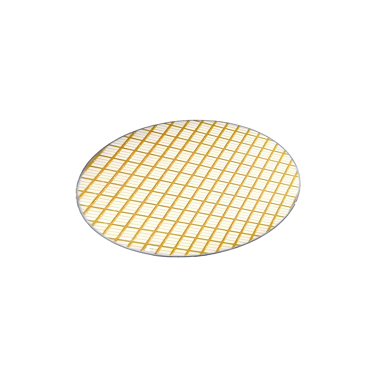
The field-stop profile is one of the most consequential structural variables in advanced IGBT wafer design. As power electronics continue to push toward higher switching frequencies and tighter thermal budgets, the way engineers shape the field-stop layer within an IGBT wafer directly determines how well the device controls minority carrier lifetime during turn-off. Even modest changes to doping concentration, layer thickness, or vertical position within the IGBT wafer can shift switching losses, affect short-circuit robustness, and alter the forward voltage drop in ways that ripple through an entire power module design.
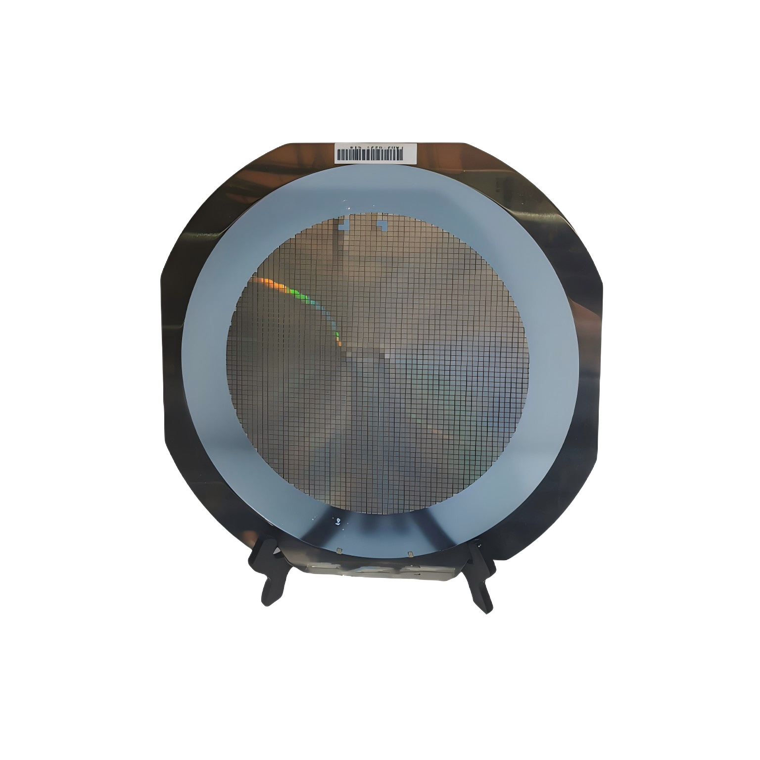
Understanding field-stop optimization in an IGBT wafer is not merely an academic exercise. Engineers working on traction drives, industrial inverters, and high-voltage power supplies depend on these structural choices to meet real-world reliability targets. This article examines the mechanisms behind field-stop behavior in an IGBT wafer, the trade-offs that arise during profile optimization, and the process considerations that allow manufacturers to achieve consistent, high-performance results across volume production of each IGBT wafer.
The Role of Field-Stop Layers in IGBT Wafer Architecture
Carrier Dynamics and the Need for a Buffer Region
A conventional punch-through IGBT wafer relies on a heavily doped buffer layer to confine the depletion region and prevent reach-through to the collector. The field-stop IGBT wafer replaces this thick, highly doped buffer with a thinner, lightly doped layer that still arrests the electric field before it reaches the collector. This architectural shift allows the IGBT wafer to be fabricated on much thinner silicon substrates, reducing conduction losses significantly. In an IGBT wafer rated for 1200 V or higher, this thinner base translates directly into lower on-state voltage and improved thermal conductivity.
The field-stop layer in an IGBT wafer must be precisely tailored so that the depletion front terminates within the layer during off-state blocking. If the field-stop doping is insufficient, the electric field can punch through the IGBT wafer and cause premature breakdown. If the doping is too heavy, excess stored charge degrades the turn-off waveform and increases tail current duration. Achieving the right balance in each IGBT wafer requires tight control over proton irradiation or diffusion processes used to form the field-stop region.
Vertical Profile Positioning Within the IGBT Wafer
The vertical position of the field-stop layer in an IGBT wafer is as important as its doping magnitude. If the layer sits too close to the collector metallization, the IGBT wafer offers minimal buffer action and risks soft breakdown behavior. If it is placed too far from the collector, the remaining collector-side silicon adds unnecessary resistivity to the IGBT wafer and raises the forward voltage drop. Simulation tools that model carrier transport within the IGBT wafer allow process engineers to explore hundreds of profile combinations before committing to a mask set, dramatically reducing development cycles for each new IGBT wafer generation.
Optimization Trade-Offs in Advanced IGBT Wafer Processing
Switching Loss Versus Conduction Loss in the IGBT Wafer
Every IGBT wafer designer faces a fundamental trade-off between switching loss and conduction loss. A field-stop profile that aggressively reduces stored charge in the IGBT wafer will accelerate turn-off, cutting switching losses at the cost of higher on-state voltage. Conversely, a softer field-stop profile in the IGBT wafer retains more charge and lowers conduction losses but extends the turn-off tail current. For a given application, the optimal IGBT wafer profile depends on the switching frequency and duty cycle. In traction inverters operating at low switching frequencies, an IGBT wafer biased toward lower conduction loss is preferable. In high-frequency industrial drives, an IGBT wafer with a sharper field-stop is often the better choice.
Proton irradiation is a widely used technique for defining the field-stop profile in an IGBT wafer because it allows precise depth targeting. By varying the proton energy during IGBT wafer processing, engineers can place recombination centers at specific depths without affecting the front-side MOS structures. Post-irradiation annealing of the IGBT wafer further refines the defect profile, offering another degree of freedom to tune the switching and conduction loss balance within each IGBT wafer batch.
Short-Circuit Robustness and Field-Stop Design in the IGBT Wafer
Short-circuit withstand time is a critical reliability metric for any IGBT wafer used in motor drive or energy conversion applications. A thin IGBT wafer with an aggressive field-stop profile may exhibit reduced short-circuit tolerance because the limited silicon volume heats up more rapidly under fault conditions. Engineers optimizing an IGBT wafer for short-circuit robustness must ensure that the field-stop layer does not prematurely collapse under the high-current, high-voltage stress of a fault event. Simulation and destructive characterization testing of the IGBT wafer are both necessary to validate robustness before a design is released to production.
Process uniformity across an entire IGBT wafer is equally important. Non-uniform field-stop implantation or annealing can produce regions of the IGBT wafer where the local device characteristics deviate significantly from the target. During module assembly, if multiple IGBT wafer dice with mismatched field-stop profiles are connected in parallel, current sharing becomes uneven, accelerating thermal aging and reducing module lifetime. Tight wafer-level process control is therefore inseparable from field-stop profile optimization in every IGBT wafer generation.
Manufacturing Process Considerations for IGBT Wafer Field-Stop Profiles
Wafer Thinning and Backside Processing in the IGBT Wafer
Modern field-stop IGBT wafer fabrication relies heavily on backside processing after front-side completion. Once the MOS cell structures on the IGBT wafer are finished, the wafer is thinned to the target thickness using mechanical grinding and chemical-mechanical polishing. This IGBT wafer thinning step must achieve excellent thickness uniformity because any bow or variation directly affects field-stop depth consistency. After thinning, the IGBT wafer receives backside implantation to form the field-stop and collector layers, followed by laser annealing to activate the dopants without damaging the front-side structures already present on the IGBT wafer.
Laser annealing of an IGBT wafer is preferred over furnace annealing in advanced nodes because the low thermal budget prevents redistribution of the lightly doped field-stop profile. Precise laser parameter control on the IGBT wafer ensures that the peak temperature at the backside is sufficient to activate implanted species without allowing heat to diffuse into the front-side MOS gate oxide. Each IGBT wafer lot must be characterized using secondary ion mass spectrometry and spreading resistance profiling to confirm that the field-stop concentration and depth match the design intent before the IGBT wafer proceeds to metallization and final testing.
Electrical Characterization and Qualification of the IGBT Wafer
After backside processing, each IGBT wafer undergoes comprehensive electrical characterization. Breakdown voltage, on-state voltage, and dynamic switching waveforms are measured across the IGBT wafer to build a statistical picture of field-stop uniformity. Any IGBT wafer lot showing excessive parameter spread is investigated to identify process root causes before the material is released. Gate charge measurements on the IGBT wafer also provide indirect evidence of field-stop effectiveness, since the tail charge during turn-off reflects how well the field-stop arrests minority carrier flow near the collector of the IGBT wafer.
FAQ
What makes the field-stop profile critical in an IGBT wafer?
The field-stop profile in an IGBT wafer controls how the depletion region terminates during blocking. It directly affects breakdown voltage, turn-off tail current, switching losses, and short-circuit robustness. A well-optimized IGBT wafer field-stop profile balances these parameters for the target application, whether that is traction, industrial drives, or renewable energy conversion.
How does proton irradiation improve IGBT wafer field-stop precision?
Proton irradiation allows engineers to place recombination centers at a defined depth within the IGBT wafer by selecting the appropriate beam energy. This depth-targeted approach gives finer control over the field-stop profile than diffusion alone. After irradiation, the IGBT wafer is annealed to stabilize the defect configuration, resulting in a predictable and reproducible field-stop characteristic across the entire IGBT wafer lot.
Why does IGBT wafer thinning affect field-stop performance?
The final thickness of the IGBT wafer sets the distance between the MOS cell structures and the collector. If the IGBT wafer is too thick, excess neutral base region increases conduction losses. If the IGBT wafer is too thin, the field-stop layer may not have adequate room to arrest the electric field, risking premature breakdown. Precise IGBT wafer thinning is therefore a prerequisite for reliable field-stop operation across all devices on the wafer.