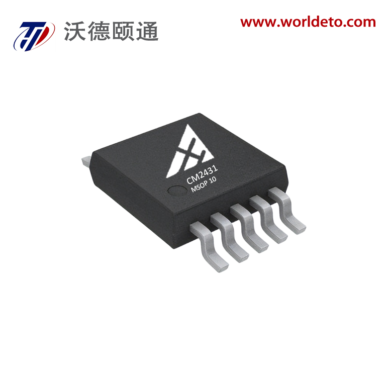
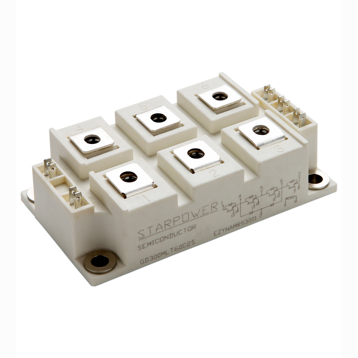
High-Performance IGBT Die Wafer Solutions - Advanced Power Semiconductor Technology

All Categories
Get a Quote

Get a Free Quote

Our representative will contact you soon.
Email
Name
Company Name
Message
0/1000

igbt die wafer

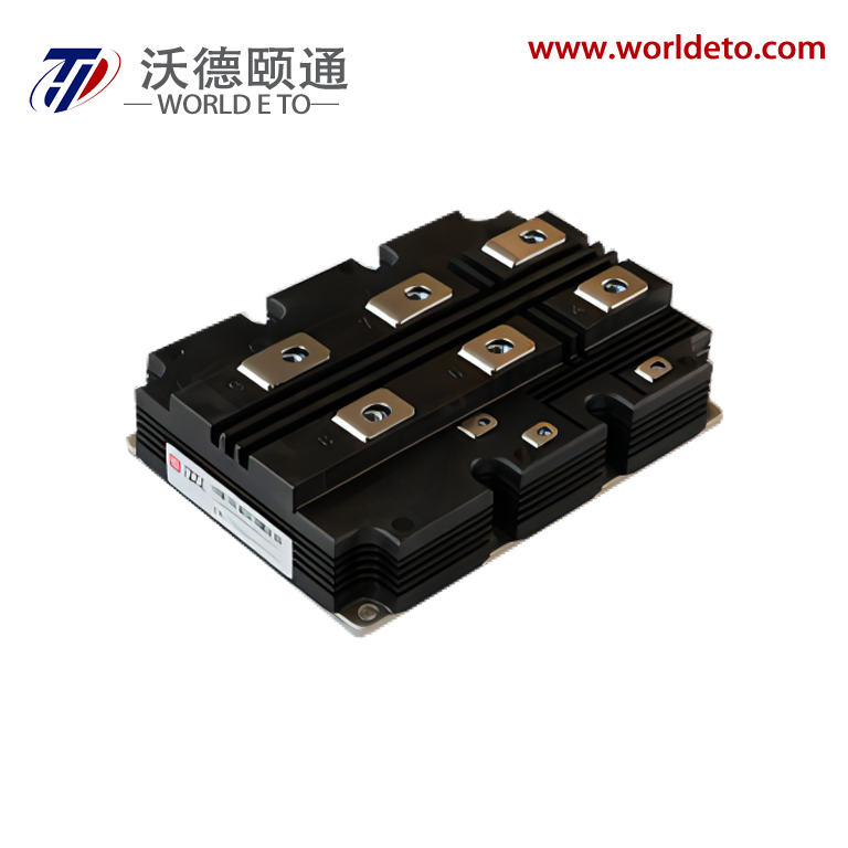
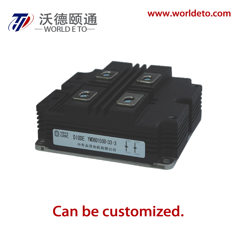
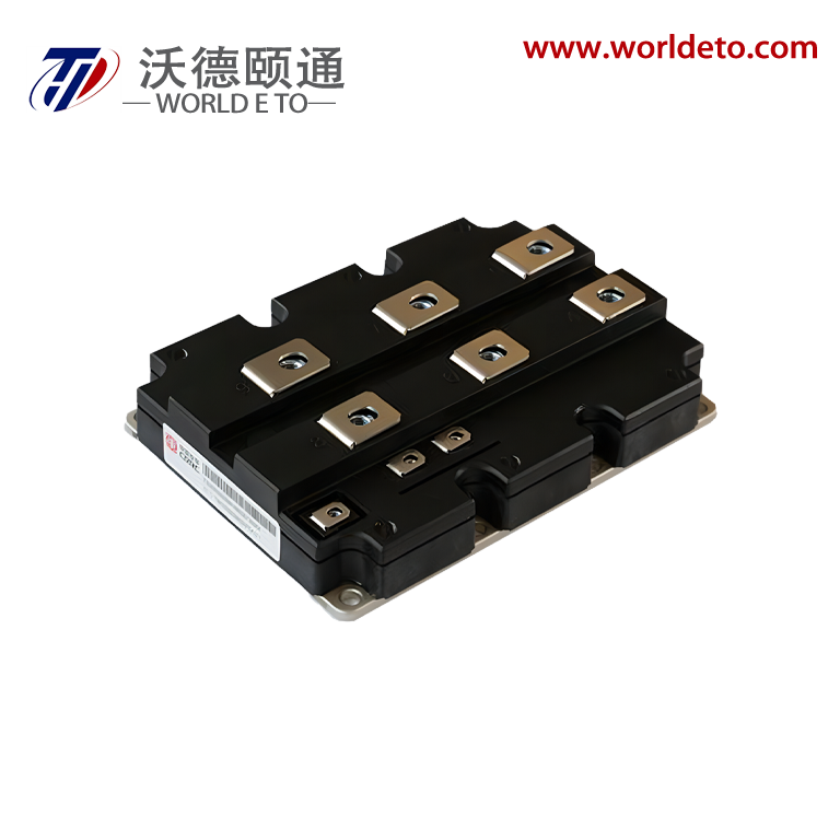
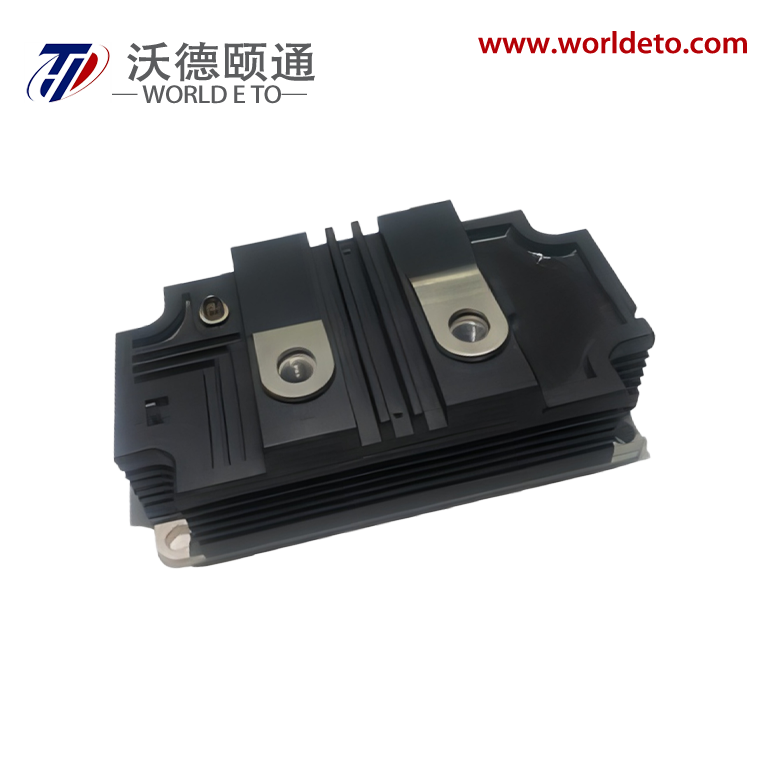
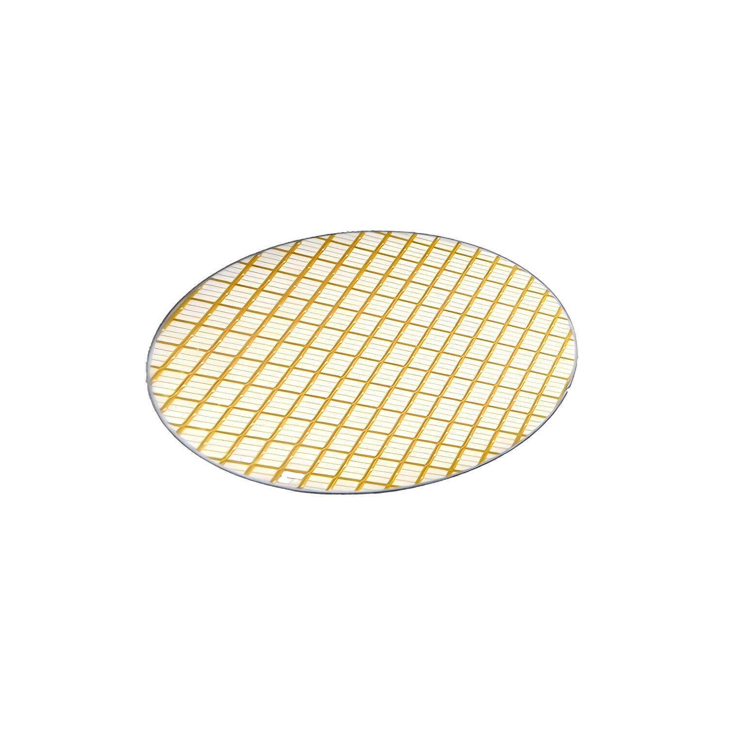
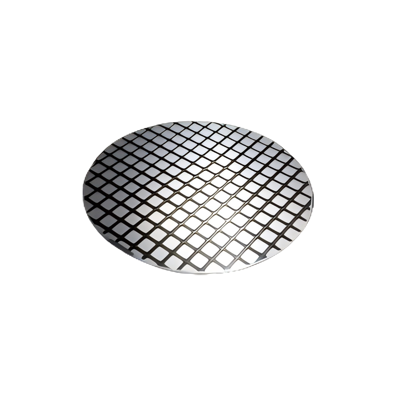
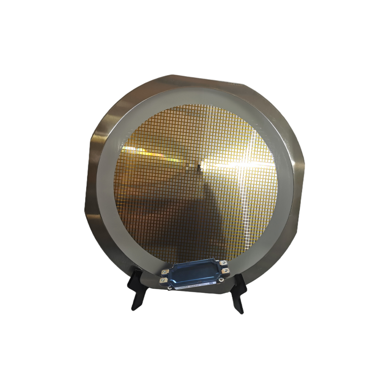
The igbt die wafer represents a crucial component in modern power electronics, serving as the foundation for Insulated Gate Bipolar Transistor technology. This semiconductor wafer combines the best characteristics of MOSFETs and bipolar junction transistors, creating a hybrid device that excels in high-power switching applications. The igbt die wafer functions as a voltage-controlled power switch, enabling efficient control of electrical current flow in various industrial and consumer applications. Its primary role involves converting and managing electrical power with minimal energy loss, making it indispensable for energy-efficient systems. The technological architecture of the igbt die wafer incorporates advanced silicon processing techniques, featuring a unique gate structure that provides superior switching capabilities. This design allows for rapid on-off transitions while maintaining excellent current-carrying capacity. The wafer's construction includes multiple layers of precisely doped silicon, creating the necessary junction configurations for optimal performance. Key technological features include low conduction losses, fast switching speeds, and robust thermal characteristics. The igbt die wafer demonstrates exceptional voltage blocking capabilities, often handling thousands of volts while maintaining stable operation. Its current density performance surpasses traditional power devices, enabling compact system designs without compromising functionality. Applications for the igbt die wafer span numerous industries, including renewable energy systems, electric vehicles, industrial motor drives, and power supply units. In solar inverters, these wafers convert DC power from panels into AC power for grid connection. Electric vehicle powertrains rely on igbt die wafers for efficient motor control and battery management. Industrial applications benefit from their reliability in variable frequency drives, welding equipment, and uninterruptible power supplies. The manufacturing process involves sophisticated clean room environments and precision fabrication techniques, ensuring consistent quality and performance across production batches.

New Product Recommendations

The igbt die wafer offers numerous practical benefits that directly impact system performance and operational costs. Energy efficiency stands as the most significant advantage, with these wafers achieving conversion efficiencies exceeding 95 percent in many applications. This high efficiency translates to reduced electricity consumption, lower operating costs, and decreased heat generation. Users experience substantial savings on energy bills while contributing to environmental sustainability through reduced power waste. The superior switching characteristics of the igbt die wafer enable faster response times compared to traditional power devices. This rapid switching capability improves system dynamic performance, allowing for better control precision in motor drives and power converters. Applications requiring quick load changes benefit enormously from this responsiveness, resulting in smoother operation and enhanced user experience. Thermal management becomes significantly easier with igbt die wafers due to their lower power dissipation. The reduced heat generation means simpler cooling systems, smaller heat sinks, and improved reliability. This thermal efficiency extends component lifespan and reduces maintenance requirements, providing long-term cost benefits for end users. System designers appreciate the compact form factor advantages that igbt die wafers provide. Their high power density allows for smaller, lighter equipment designs without sacrificing performance. This miniaturization benefit proves especially valuable in space-constrained applications like electric vehicles and portable equipment. The robust construction of igbt die wafers ensures reliable operation under demanding conditions. They withstand voltage spikes, temperature fluctuations, and electrical stress better than alternative technologies. This durability reduces system downtime and maintenance costs, improving overall return on investment. Cost-effectiveness emerges through multiple factors including reduced component count, simplified circuit designs, and lower system complexity. The igbt die wafer often replaces multiple discrete components, streamlining manufacturing and reducing assembly costs. Additionally, their wide operating voltage and current ranges provide design flexibility, allowing engineers to use fewer device variants across different applications. Installation and integration prove straightforward due to standard packaging options and well-established design practices, reducing development time and accelerating time-to-market for new products.

Latest News

High-Accuracy ADC & DAC Chips: The Core of Precision Measurement Systems

07

Jan

High-Accuracy ADC & DAC Chips: The Core of Precision Measurement Systems

In today's advanced measurement and control systems, the bridge between analog real-world signals and digital processing relies heavily on specialized semiconductor components. These critical interface chips, specifically High-Accuracy ADC & DAC Chip...
View More
Building Reliable Systems: The Role of Precision Voltage References and LDOs in Industrial Applications

07

Jan

Building Reliable Systems: The Role of Precision Voltage References and LDOs in Industrial Applications

Industrial automation and control systems demand unwavering accuracy and reliability to ensure optimal performance across diverse operating conditions. At the heart of these sophisticated systems lie critical components that provide stable power mana...
View More
From ADC to LDO: Complete High-Precision, Low-Power Domestic Chip Replacement Solutions

02

Feb

From ADC to LDO: Complete High-Precision, Low-Power Domestic Chip Replacement Solutions

The semiconductor industry faces unprecedented challenges as global supply chain disruptions and geopolitical tensions drive demand for reliable domestic chip replacement solutions. Companies across industries are increasingly seeking alternatives to...
View More
The Best Domestic Alternatives for High-Performance ADC and DAC Chips in 2026

03

Feb

The Best Domestic Alternatives for High-Performance ADC and DAC Chips in 2026

The semiconductor industry is experiencing unprecedented demand for high-performance analog-to-digital converter and digital-to-analog converter solutions, driving engineers and procurement teams to seek reliable domestic alternatives for ADC and DAC...
View More

Get a Free Quote

Our representative will contact you soon.
Email
Name
Company Name
Message
0/1000

igbt die wafer

Superior Power Handling and Efficiency Performance

Superior Power Handling and Efficiency Performance

The igbt die wafer delivers exceptional power handling capabilities that surpass conventional power semiconductor technologies, making it the preferred choice for high-performance applications. This superior performance stems from the innovative hybrid design that combines the voltage control advantages of MOSFETs with the current-carrying capabilities of bipolar transistors. The result is a device that handles substantial power levels while maintaining impressive efficiency ratings. In practical terms, users benefit from reduced energy consumption and lower operating temperatures, which directly translate to cost savings and improved system reliability. The power handling excellence of the igbt die wafer becomes evident in applications requiring kilowatt to megawatt power levels. Industrial motor drives utilizing these wafers can control massive machinery with precision while consuming minimal control power. The voltage blocking capability often exceeds several thousand volts, enabling direct connection to medium-voltage systems without additional isolation components. This high-voltage capability simplifies system architecture and reduces component count, lowering both initial costs and maintenance requirements. Current density performance represents another crucial advantage, with modern igbt die wafers supporting hundreds of amperes in compact packages. This high current density enables smaller system footprints while maintaining full power capability, particularly valuable in space-critical applications like electric vehicle inverters and renewable energy converters. The switching losses remain remarkably low even at high frequencies, allowing for more efficient power conversion and reduced cooling requirements. Efficiency levels consistently exceed 95 percent in well-designed applications, with some implementations achieving 98 percent efficiency. This exceptional efficiency reduces waste heat generation, simplifies thermal management, and extends component lifespan. The environmental benefits include reduced carbon footprint and lower energy costs, making igbt die wafer technology attractive for sustainable energy applications. Real-world testing demonstrates that systems incorporating these wafers often achieve 10-15 percent better efficiency compared to alternative technologies, resulting in significant operational savings over the product lifetime.
Advanced Switching Speed and Control Precision

Advanced Switching Speed and Control Precision

The igbt die wafer excels in switching speed performance, offering rapid transition times that enhance system responsiveness and control accuracy. This advanced switching capability results from sophisticated gate structure design and optimized semiconductor physics that minimize switching delays and reduce transition losses. The practical benefits manifest as improved dynamic response, better regulation accuracy, and enhanced system stability across varying load conditions. Users experience smoother operation, reduced electromagnetic interference, and more precise control over their applications. Switching speeds measured in nanoseconds enable high-frequency operation that was previously impossible with traditional power devices. This fast switching allows for smaller passive components like inductors and capacitors, reducing overall system size and weight. High-frequency operation also improves regulation response, enabling tighter control loops and better disturbance rejection. Applications requiring rapid load changes, such as servo drives and high-performance motor controls, benefit enormously from this switching speed advantage. The turn-on and turn-off characteristics of the igbt die wafer are carefully optimized to minimize switching losses while maintaining safe operation. Advanced gate drive techniques further enhance performance, allowing users to tailor switching speed to specific application requirements. This flexibility enables optimization for either maximum efficiency or fastest response time, depending on system priorities. The low switching losses contribute significantly to overall system efficiency and thermal management. Control precision reaches new levels with igbt die wafers due to their excellent linearity and predictable characteristics. The gate voltage directly controls output current with minimal variation across temperature and aging effects. This predictability simplifies control system design and improves long-term stability. Manufacturing consistency ensures that devices from the same production batch exhibit nearly identical characteristics, facilitating parallel operation and simplified control strategies. The electromagnetic compatibility benefits from clean switching transitions that minimize conducted and radiated emissions. This cleaner switching reduces filter requirements and simplifies compliance with electromagnetic interference regulations, saving costs and design complexity in noise-sensitive applications.
Exceptional Reliability and Temperature Performance

Exceptional Reliability and Temperature Performance

The igbt die wafer demonstrates outstanding reliability characteristics that ensure dependable operation in challenging environments and demanding applications. This exceptional reliability stems from robust semiconductor design, advanced packaging technologies, and rigorous quality control processes that eliminate potential failure modes. Users benefit from extended equipment lifetimes, reduced maintenance costs, and improved system availability. The reliability advantage becomes particularly valuable in mission-critical applications where downtime carries significant costs or safety implications. Temperature performance represents a key reliability factor, with igbt die wafers operating reliably across wide temperature ranges from sub-zero to over 175 degrees Celsius junction temperatures. This broad temperature capability eliminates the need for complex environmental controls in many applications, reducing system complexity and costs. The thermal cycling resistance ensures stable operation through repeated heating and cooling cycles without performance degradation or premature failure. Applications in automotive, aerospace, and industrial environments benefit greatly from this temperature robustness. The avalanche energy capability of modern igbt die wafers provides protection against voltage spikes and transient events that could damage conventional devices. This built-in ruggedness simplifies protection circuit design and improves system fault tolerance. Short circuit withstand capability further enhances reliability by allowing brief overcurrent conditions without device failure, providing valuable protection during system faults or abnormal operating conditions. Manufacturing quality control ensures consistent device parameters and long-term stability through comprehensive testing and screening processes. Statistical quality control methods identify and eliminate potential reliability risks before devices reach customers. Accelerated aging tests verify long-term performance characteristics, providing confidence in extended operational lifetimes. Many igbt die wafer applications demonstrate operational lifetimes exceeding 20 years with proper application design and thermal management. The failure rate statistics show significant improvements over alternative technologies, with mean time between failures often exceeding 100,000 hours in properly designed systems. This reliability translates directly to reduced warranty costs, improved customer satisfaction, and lower total cost of ownership. Predictive maintenance capabilities enable condition monitoring and proactive replacement scheduling, further enhancing system reliability and reducing unexpected failures.

Get a Free Quote

Our representative will contact you soon.
Email
Name
Company Name
Message
0/1000