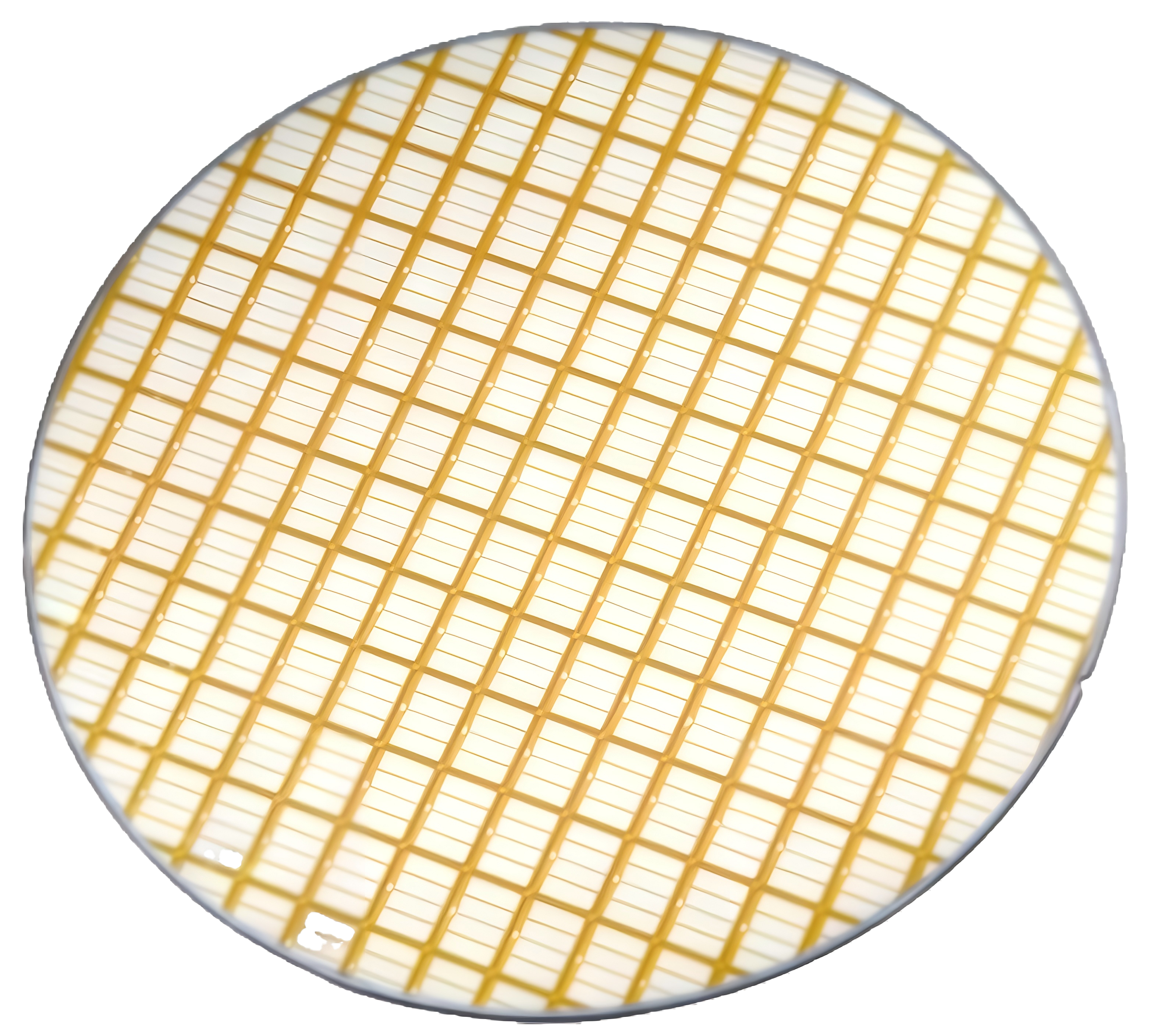
Established Supply Chain and Industry Standardization Benefits
The 12 inch wafer benefits from a mature and well-established global supply chain infrastructure that provides manufacturers with reliable access to high-quality substrates, supporting materials, and specialized processing equipment. This standardization has created a robust ecosystem of suppliers, equipment manufacturers, and service providers all focused on 12 inch wafer technology, resulting in competitive pricing, consistent availability, and continuous technological improvements. The widespread adoption of the 12 inch wafer format has driven significant investments in manufacturing capacity worldwide, ensuring stable supply even during periods of high demand and enabling manufacturers to scale production volumes confidently. Equipment standardization around the 12 inch wafer format provides substantial advantages in terms of technology transfer, process development, and manufacturing flexibility, as proven processes can be readily implemented across different facilities and production lines. The extensive installed base of 12 inch wafer processing equipment creates opportunities for equipment sharing, collaborative development programs, and technology licensing agreements that accelerate innovation and reduce development costs for semiconductor manufacturers. Industry standardization has also facilitated the development of comprehensive quality standards, testing protocols, and certification procedures specifically for 12 inch wafer production, ensuring consistent quality levels across different suppliers and geographic regions. The mature supply chain includes specialized logistics networks optimized for 12 inch wafer transportation, with custom packaging solutions, handling procedures, and shipping methods that minimize contamination risks and physical damage during transit. Raw material suppliers have optimized their production processes specifically for 12 inch wafer requirements, resulting in improved silicon purity, better crystal quality, and more consistent material properties that enhance device performance and manufacturing yields. The established infrastructure enables rapid technology adoption and process improvements, as new innovations can leverage existing equipment platforms and supply relationships rather than requiring completely new manufacturing ecosystems, significantly reducing implementation timelines and associated risks for manufacturers adopting advanced semiconductor technologies.