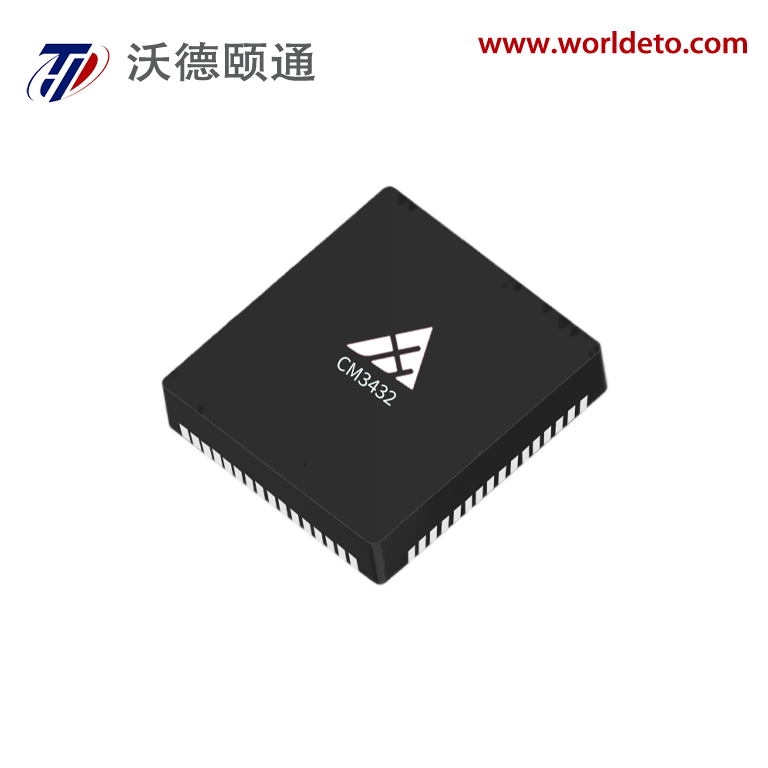
High Speed ADC IC - Ultra-Fast Analog to Digital Conversion Solutions

All Categories
Get a Quote

Get a Free Quote

Our representative will contact you soon.
Email
Name
Company Name
Message
0/1000

high speed adc ic

A high speed ADC IC represents a sophisticated analog-to-digital converter integrated circuit designed to transform continuous analog signals into discrete digital values at exceptionally rapid sampling rates. These specialized semiconductor devices operate at frequencies ranging from hundreds of megahertz to several gigahertz, making them essential components in modern electronic systems requiring precise signal processing capabilities. The high speed ADC IC employs advanced conversion architectures such as flash, pipeline, or successive approximation register designs to achieve optimal performance characteristics. These integrated circuits feature multiple input channels, programmable gain amplifiers, and sophisticated timing control mechanisms that ensure accurate signal capture across diverse operating conditions. The technological foundation of high speed ADC IC relies on cutting-edge CMOS fabrication processes, often utilizing specialized bipolar or BiCMOS technologies to maximize conversion speeds while maintaining exceptional linearity and dynamic range performance. Modern high speed ADC IC designs incorporate advanced calibration algorithms, digital error correction techniques, and temperature compensation features that guarantee consistent performance across varying environmental conditions. These devices typically offer resolution ranges from 8-bit to 16-bit configurations, with sampling rates exceeding 1 GSPS in premium implementations. The high speed ADC IC integrates essential supporting circuitry including voltage references, clock generation systems, and digital output drivers within a single package, significantly reducing external component requirements and system complexity. Applications for high speed ADC IC span across telecommunications infrastructure, radar systems, medical imaging equipment, oscilloscopes, software-defined radio platforms, and high-frequency measurement instruments. The versatility of high speed ADC IC enables engineers to implement sophisticated signal processing solutions in compact form factors while maintaining exceptional performance standards. These integrated circuits support various industry-standard interfaces including LVDS, JESD204B, and parallel output formats, ensuring seamless integration with existing system architectures and enabling efficient data transfer to downstream processing elements.

New Product Recommendations

High speed ADC IC delivers exceptional performance benefits that directly translate into improved system capabilities and operational efficiency for end-users. The primary advantage lies in the superior sampling rates these devices achieve, enabling accurate capture of high-frequency signals that conventional converters cannot handle effectively. This capability proves crucial for applications requiring real-time signal analysis, where missing critical information due to inadequate sampling rates can compromise entire system functionality. The integrated design approach of high speed ADC IC significantly reduces board space requirements compared to discrete component solutions, allowing engineers to create more compact and portable equipment while maintaining superior performance standards. Cost benefits emerge through reduced component count, simplified PCB layouts, and decreased manufacturing complexity, resulting in lower overall system costs and improved profit margins for equipment manufacturers. Power efficiency represents another significant advantage, as modern high speed ADC IC implementations utilize advanced power management techniques and optimized circuit topologies to minimize energy consumption without sacrificing performance. These devices incorporate sophisticated noise reduction technologies and exceptional signal-to-noise ratio characteristics, ensuring clean digital output even in challenging electromagnetic environments. The reliability factor of high speed ADC IC surpasses discrete solutions through comprehensive testing, qualification processes, and integrated protection features that guard against overvoltage conditions and thermal stress. Flexibility advantages include programmable gain settings, configurable input ranges, and software-controlled operating parameters that allow single device types to serve multiple application requirements. The high speed ADC IC offers superior linearity performance across the entire input range, minimizing harmonic distortion and spurious signals that could degrade system accuracy. Integration benefits extend to reduced design time, simplified inventory management, and improved supply chain efficiency for manufacturers utilizing these components. Quality assurance advantages include comprehensive factory calibration, built-in self-test capabilities, and extensive characterization data that enable predictable performance outcomes. The standardized interfaces and proven compatibility of high speed ADC IC with popular digital signal processors and FPGA platforms streamline system development processes and reduce time-to-market requirements for new products.

Tips And Tricks

Is Your ADC/DAC Underperforming? The Culprit Could Be Your Voltage Reference

24

Nov

Is Your ADC/DAC Underperforming? The Culprit Could Be Your Voltage Reference

In the realm of precision analog-to-digital and digital-to-analog conversion, engineers often focus on the specifications of the ADC or DAC itself while overlooking a critical component that can make or break system performance. The voltage reference...
View More
Building Reliable Systems: The Role of Precision Voltage References and LDOs in Industrial Applications

07

Jan

Building Reliable Systems: The Role of Precision Voltage References and LDOs in Industrial Applications

Industrial automation and control systems demand unwavering accuracy and reliability to ensure optimal performance across diverse operating conditions. At the heart of these sophisticated systems lie critical components that provide stable power mana...
View More
Low-Power, High-Precision: How Domestic Linear Regulators and Voltage References Enable Import Substitution

02

Feb

Low-Power, High-Precision: How Domestic Linear Regulators and Voltage References Enable Import Substitution

The global semiconductor supply chain disruptions of recent years have highlighted the critical importance of developing robust domestic manufacturing capabilities. As industries worldwide grapple with component shortages and geopolitical tensions, t...
View More
Domestic High-Precision Linear Regulators and Instrumentation Amplifiers: Low-Power Design for Replacing Imported Chips

02

Feb

Domestic High-Precision Linear Regulators and Instrumentation Amplifiers: Low-Power Design for Replacing Imported Chips

The semiconductor industry has witnessed a significant shift toward domestically manufactured components, particularly in the realm of precision analog circuits. Domestic high-precision linear regulators have emerged as crucial components for enginee...
View More

Get a Free Quote

Our representative will contact you soon.
Email
Name
Company Name
Message
0/1000

high speed adc ic

Ultra-Fast Sampling Capabilities Enable Real-Time Signal Processing

Ultra-Fast Sampling Capabilities Enable Real-Time Signal Processing

The high speed ADC IC delivers unprecedented sampling rates that revolutionize how engineers approach signal acquisition and processing challenges in demanding applications. These advanced integrated circuits achieve sampling frequencies exceeding 1 billion samples per second, enabling precise capture of high-frequency analog signals that traditional converters simply cannot handle effectively. The ultra-fast sampling capability proves essential for applications such as radar signal processing, where split-second timing accuracy determines system effectiveness and operational success. Modern high speed ADC IC designs employ sophisticated clock generation and distribution networks that maintain precise timing relationships across multiple channels, ensuring coherent sampling even at extreme frequencies. The sampling accuracy remains consistent across the entire operating frequency range, with minimal aperture jitter and excellent clock-to-output timing specifications that guarantee reliable performance in critical applications. Engineers benefit from the ability to capture transient events, analyze high-speed digital communications signals, and perform real-time spectrum analysis without compromising signal integrity or missing crucial information. The high speed ADC IC incorporates advanced track-and-hold amplifiers with exceptional bandwidth characteristics, enabling accurate acquisition of signals with rapid slew rates and complex modulation schemes. These capabilities prove particularly valuable in software-defined radio applications, where wide bandwidth signals require simultaneous capture and processing across multiple frequency bands. The sampling architecture of high speed ADC IC supports both single-shot and continuous acquisition modes, providing flexibility for diverse measurement scenarios and system requirements. Quality assurance measures include comprehensive linearity testing, spurious-free dynamic range verification, and extensive characterization across temperature and supply voltage variations. The result is a high speed ADC IC solution that enables engineers to push the boundaries of signal processing performance while maintaining the reliability and consistency required for mission-critical applications.
Exceptional Integration Reduces System Complexity and Cost

Exceptional Integration Reduces System Complexity and Cost

The high speed ADC IC represents a paradigm shift toward comprehensive integration that dramatically simplifies system design while reducing overall costs and improving reliability. Unlike discrete component approaches that require extensive external circuitry, the high speed ADC IC incorporates essential analog front-end components, precision voltage references, clock generation systems, and digital interface logic within a single integrated package. This integration approach eliminates the need for multiple external components, reducing PCB real estate requirements by up to 70 percent compared to equivalent discrete solutions. The cost benefits extend beyond component savings to include reduced assembly time, simplified inventory management, and decreased testing requirements during manufacturing processes. Engineers appreciate the simplified design process enabled by high speed ADC IC integration, as pre-characterized and optimized internal circuitry eliminates lengthy design iterations and component matching procedures. The integrated voltage reference system maintains exceptional stability and low temperature coefficient performance, ensuring consistent conversion accuracy without requiring expensive external reference components. Clock generation and distribution networks within the high speed ADC IC provide clean, low-jitter timing signals that optimize conversion performance while eliminating external clock conditioning requirements. The comprehensive integration includes sophisticated power management features that optimize current consumption based on operating conditions, extending battery life in portable applications and reducing thermal management challenges. Quality benefits emerge through factory calibration of integrated components, comprehensive testing of internal signal paths, and guaranteed performance specifications that eliminate uncertainty associated with discrete component variations. The high speed ADC IC integration approach enables predictable performance outcomes, simplified procurement processes, and reduced supply chain complexity for equipment manufacturers. Reliability improvements result from eliminating numerous solder joints, reducing component count, and minimizing potential failure points within the signal acquisition chain. The standardized footprint and pinout configurations of high speed ADC IC products facilitate design reuse across multiple product platforms, further reducing development costs and time-to-market requirements.
Superior Signal Fidelity Ensures Accurate Digital Representation

Superior Signal Fidelity Ensures Accurate Digital Representation

The high speed ADC IC delivers exceptional signal fidelity through advanced analog circuit design techniques and sophisticated digital processing algorithms that preserve signal integrity throughout the conversion process. These integrated circuits achieve outstanding spurious-free dynamic range performance, typically exceeding 80 dB across the full Nyquist bandwidth, ensuring that unwanted harmonic content and conversion artifacts remain well below the noise floor. The superior linearity characteristics of high speed ADC IC result from carefully optimized analog front-end architectures, precision component matching, and comprehensive factory calibration procedures that minimize differential and integral nonlinearity errors. Advanced error correction techniques integrated within the high speed ADC IC automatically compensate for process variations, temperature effects, and aging-related parameter drift, maintaining consistent performance throughout the operational lifetime. The exceptional signal-to-noise ratio performance enables accurate digitization of low-level signals while preserving dynamic range for high-amplitude inputs, making these devices ideal for demanding measurement and communication applications. Sophisticated anti-aliasing filter integration within the high speed ADC IC prevents unwanted frequency components from corrupting the digital output, ensuring clean spectral content and reliable signal analysis results. The wide input bandwidth capability accommodates signals with complex modulation schemes and rapid transition characteristics without introducing distortion or limiting system performance. Temperature stability features include comprehensive thermal compensation algorithms and optimized circuit topologies that maintain conversion accuracy across industrial temperature ranges. The high speed ADC IC incorporates advanced sampling techniques such as randomized sampling clocks and dither injection that effectively reduce quantization noise and improve effective resolution for specific signal types. Power supply rejection performance exceeds industry standards through integrated filtering and regulation circuits that isolate sensitive analog sections from digital switching noise and external interference sources. The combination of exceptional analog performance and sophisticated digital processing within the high speed ADC IC enables engineers to achieve measurement accuracy levels previously possible only with expensive laboratory instruments.

Get a Free Quote

Our representative will contact you soon.
Email
Name
Company Name
Message
0/1000