High-Performance Analog to Digital Converter IC Solutions - Precision Signal Conversion Technology

All Categories
Get a Quote

Get a Free Quote

Our representative will contact you soon.
Email
Name
Company Name
Message
0/1000

analog to digital converter ic

An analog to digital converter IC represents a fundamental semiconductor component that bridges the gap between analog signals from the real world and digital processing systems. This integrated circuit captures continuous analog voltages and transforms them into discrete digital values that microprocessors, computers, and digital systems can interpret and manipulate. The analog to digital converter IC serves as the essential interface in countless electronic devices, enabling everything from smartphone audio recording to industrial automation systems. Modern analog to digital converter IC designs incorporate sophisticated signal processing architectures that deliver exceptional precision and speed. These chips typically feature multiple input channels, programmable gain amplifiers, and advanced sampling techniques that ensure accurate signal conversion across various operating conditions. The resolution of an analog to digital converter IC determines its ability to distinguish between small voltage differences, with common resolutions ranging from 8-bit to 24-bit configurations. Higher resolution analog to digital converter IC units provide finer granularity in signal representation, making them ideal for precision measurement applications. The sampling rate specification indicates how frequently the analog to digital converter IC can perform conversions, with high-speed variants capable of millions of samples per second. These components integrate advanced calibration circuits that compensate for temperature variations and aging effects, maintaining consistent performance throughout their operational lifetime. The analog to digital converter IC incorporates sophisticated anti-aliasing filters and noise reduction techniques that preserve signal integrity during the conversion process. Many modern designs feature built-in reference voltage sources, reducing external component requirements and simplifying circuit implementation. The power consumption characteristics of analog to digital converter IC technology have improved significantly, with low-power variants extending battery life in portable applications while maintaining conversion accuracy.

New Products

The primary advantage of implementing an analog to digital converter IC lies in its ability to eliminate noise and signal degradation that typically plague analog signal processing chains. Digital signals remain immune to electromagnetic interference and environmental factors that can corrupt analog transmissions, ensuring reliable data integrity across extended distances and harsh operating environments. This analog to digital converter IC capability translates directly into improved system reliability and reduced maintenance requirements for end users. Cost efficiency represents another significant benefit, as analog to digital converter IC technology integrates multiple complex functions into a single semiconductor package, reducing component count and assembly complexity. This integration eliminates the need for discrete operational amplifiers, reference circuits, and timing components, substantially lowering overall system costs while improving manufacturability. The space-saving characteristics of analog to digital converter IC designs enable compact product development, particularly valuable in portable electronics and embedded systems where board space remains at a premium. Flexibility stands out as a key advantage, with programmable analog to digital converter IC variants allowing users to configure conversion parameters, input ranges, and sampling rates through software control. This adaptability enables a single analog to digital converter IC to serve multiple applications, reducing inventory requirements and development time. The precision capabilities of modern analog to digital converter IC technology surpass traditional analog measurement techniques, providing repeatable and accurate results that remain consistent across temperature variations and time. Digital processing advantages become immediately accessible once signals pass through an analog to digital converter IC, enabling advanced mathematical operations, filtering, and analysis that would be impossible or impractical with analog circuits. Power efficiency improvements in contemporary analog to digital converter IC designs support battery-powered applications, with many variants offering shutdown modes and adjustable power consumption based on performance requirements. The diagnostic capabilities built into advanced analog to digital converter IC units provide real-time monitoring of conversion quality and system health, enabling predictive maintenance and early fault detection. Standardized digital interfaces simplify system integration, as analog to digital converter IC outputs connect directly to microcontrollers, DSPs, and communication protocols without requiring additional level conversion or signal conditioning circuits.

Practical Tips

Low-Power Design Secrets: Utilizing Precision LDOs and Voltage References for Extended Battery Life

07

Jan

Low-Power Design Secrets: Utilizing Precision LDOs and Voltage References for Extended Battery Life

Modern electronic systems demand increasingly sophisticated power management strategies to achieve extended battery life while maintaining optimal performance. The integration of precision LDOs and voltage references has become a cornerstone of effic...
View More
Domestic High-Precision Linear Regulators and Instrumentation Amplifiers: Low-Power Design for Replacing Imported Chips

02

Feb

Domestic High-Precision Linear Regulators and Instrumentation Amplifiers: Low-Power Design for Replacing Imported Chips

The semiconductor industry has witnessed a significant shift toward domestically manufactured components, particularly in the realm of precision analog circuits. Domestic high-precision linear regulators have emerged as crucial components for enginee...
View More
The Best Domestic Alternatives for High-Performance ADC and DAC Chips in 2026

03

Feb

The Best Domestic Alternatives for High-Performance ADC and DAC Chips in 2026

The semiconductor industry is experiencing unprecedented demand for high-performance analog-to-digital converter and digital-to-analog converter solutions, driving engineers and procurement teams to seek reliable domestic alternatives for ADC and DAC...
View More
Breaking Speed Barriers: The Future of High-Speed ADCs in Modern Communication

03

Feb

Breaking Speed Barriers: The Future of High-Speed ADCs in Modern Communication

The telecommunications industry continues to push the boundaries of data transmission speeds, driving unprecedented demand for advanced analog-to-digital conversion technologies. High-speed ADCs have emerged as the cornerstone of modern communication...
View More

Get a Free Quote

Our representative will contact you soon.
Email
Name
Company Name
Message
0/1000

analog to digital converter ic

Superior Signal Processing Architecture

Superior Signal Processing Architecture

The advanced signal processing architecture embedded within modern analog to digital converter IC designs delivers unprecedented performance through sophisticated engineering innovations that address real-world measurement challenges. These integrated circuits incorporate multi-stage signal conditioning paths that optimize input signals before conversion, including programmable gain amplifiers that automatically adjust signal levels to match the optimal input range of the analog to digital converter IC core. This intelligent preprocessing capability ensures maximum resolution utilization regardless of input signal amplitude variations, delivering consistent accuracy across diverse operating scenarios. The analog to digital converter IC architecture features advanced oversampling techniques combined with digital filtering that effectively increases the signal-to-noise ratio beyond what traditional sampling methods can achieve. This approach allows the analog to digital converter IC to extract weak signals from noisy environments, making it invaluable for precision measurement applications where signal integrity is paramount. The implementation of delta-sigma modulation in high-end analog to digital converter IC designs provides exceptional linearity and low distortion characteristics that surpass successive approximation or flash conversion methods. Temperature compensation circuits integrated within the analog to digital converter IC automatically adjust conversion parameters based on thermal conditions, maintaining calibrated accuracy across the full operating temperature range without requiring external calibration procedures. The sophisticated timing control systems ensure precise sample acquisition timing, eliminating aperture jitter and sample-and-hold errors that could degrade conversion accuracy. Built-in self-test capabilities allow the analog to digital converter IC to continuously monitor its own performance, detecting drift or degradation before it impacts measurement quality. This proactive approach to quality assurance provides users with confidence in their measurement results while enabling predictive maintenance strategies that minimize downtime. The flexible input multiplexing capabilities of advanced analog to digital converter IC designs allow simultaneous monitoring of multiple signal sources through a single converter, reducing system complexity and cost while maintaining individual channel isolation and accuracy.
Exceptional Accuracy and Resolution Performance

Exceptional Accuracy and Resolution Performance

The exceptional accuracy and resolution performance of contemporary analog to digital converter IC technology stems from breakthrough semiconductor fabrication techniques and innovative circuit design methodologies that push the boundaries of measurement precision. These integrated circuits achieve resolution specifications that were previously impossible with discrete component implementations, with some analog to digital converter IC variants reaching 24-bit resolution that can distinguish voltage differences smaller than microvolts. This extraordinary precision capability opens new possibilities for scientific instrumentation, medical devices, and industrial process control applications where minute signal variations carry critical information. The analog to digital converter IC maintains this high resolution performance across its full input range through careful attention to linearity specifications, ensuring that each digital code corresponds precisely to its intended analog voltage level. Advanced calibration algorithms embedded within the analog to digital converter IC continuously optimize conversion parameters, compensating for component variations and environmental factors that could introduce measurement errors. The temperature coefficient specifications of premium analog to digital converter IC designs demonstrate remarkable stability, with drift rates measured in parts per million per degree Celsius, ensuring consistent accuracy across industrial temperature ranges. Noise performance represents another critical aspect of analog to digital converter IC excellence, with effective number of bits (ENOB) ratings that approach theoretical limits through sophisticated noise reduction techniques and careful analog front-end design. The spurious-free dynamic range (SFDR) characteristics of high-performance analog to digital converter IC units enable accurate measurement of signals in the presence of strong interfering frequencies, crucial for communications and spectrum analysis applications. Input impedance matching capabilities ensure that the analog to digital converter IC does not load the signal source, preserving measurement accuracy for high-impedance sensors and precision voltage references. The conversion speed versus accuracy trade-offs in analog to digital converter IC designs have been optimized through advanced architectures that maintain high resolution even at elevated sampling rates, enabling real-time processing of precision measurements without sacrificing quality.
Seamless Integration and Connectivity Features

Seamless Integration and Connectivity Features

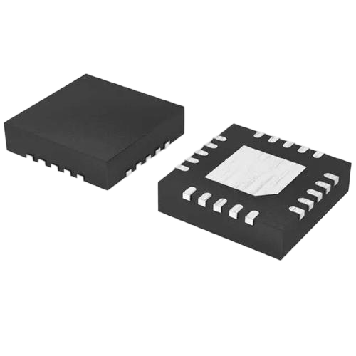
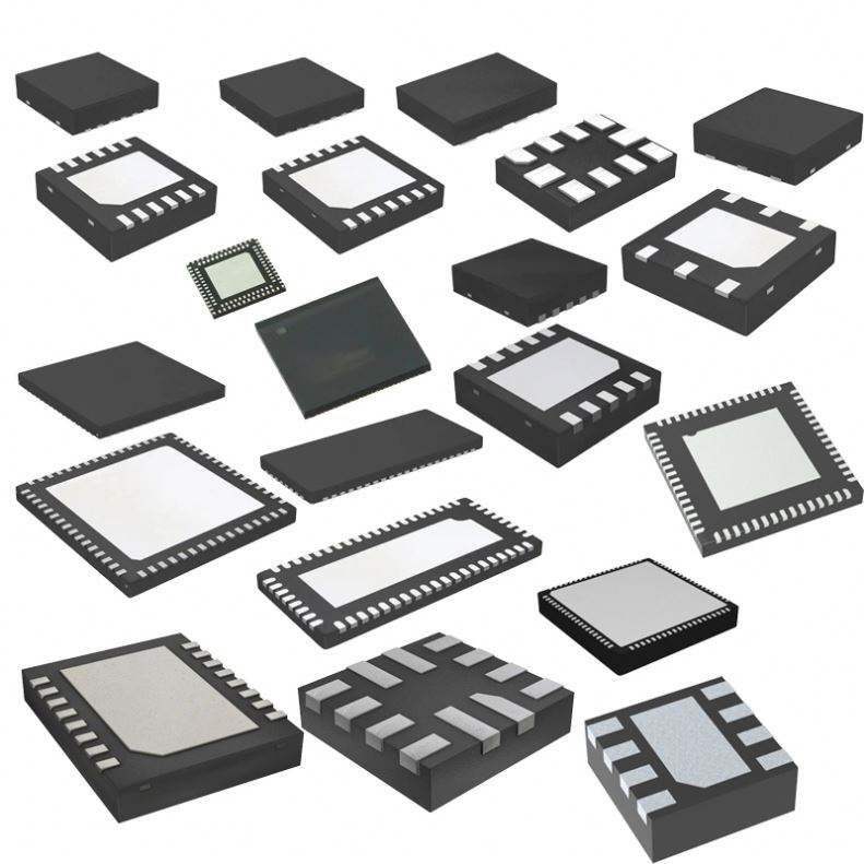
The seamless integration and connectivity features built into modern analog to digital converter IC designs revolutionize system development by providing comprehensive interface options and intelligent communication capabilities that streamline implementation processes. These integrated circuits incorporate standard digital communication protocols including SPI, I2C, and parallel interfaces that connect directly to microcontrollers and digital signal processors without requiring additional interface circuitry. The analog to digital converter IC features sophisticated command structures that allow host processors to configure conversion parameters, trigger measurements, and retrieve results through simple software commands, eliminating the need for complex timing control circuits. Advanced analog to digital converter IC variants include built-in FIFOs and data buffering capabilities that prevent data loss during high-speed continuous conversion operations, particularly valuable in data acquisition systems where consistent sampling intervals are critical. The interrupt and alarm generation capabilities of intelligent analog to digital converter IC designs provide real-time notification of conversion completion, threshold violations, or fault conditions, enabling responsive system behavior without continuous polling overhead. Power management integration represents a significant advancement, with analog to digital converter IC units offering multiple power modes that can be dynamically controlled based on system requirements, extending battery life in portable applications while maintaining conversion availability when needed. The analog to digital converter IC incorporates comprehensive diagnostic and status reporting features that provide detailed information about conversion quality, input conditions, and internal operating parameters, supporting advanced system monitoring and maintenance strategies. Flexible triggering options allow the analog to digital converter IC to synchronize conversions with external events, enabling precise timing relationships in multi-channel data acquisition systems and synchronized measurement applications. The standardized footprints and pinout configurations of analog to digital converter IC families simplify PCB design and enable easy performance upgrades without requiring circuit board modifications. Advanced analog to digital converter IC designs include built-in voltage references and bias generation circuits that eliminate external component dependencies, reducing bill of materials costs and improving system reliability through integration of precision reference sources that maintain stability across temperature and supply voltage variations.

Get a Free Quote

Our representative will contact you soon.
Email
Name
Company Name
Message
0/1000