
 EN
EN
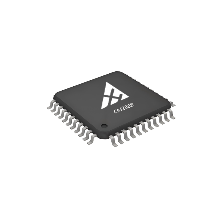
Modern industrial systems demand unprecedented efficiency in signal processing, and low-power data acquisition has become the defining benchmark for next-generation measurement infrastructure. As sensor networks proliferate across manufacturing facilities, research laboratories, and edge computing environments, the ability to capture high-fidelity analog signals while minimizing energy consumption directly impacts operational costs and system longevity. Ultra-high-speed analog-to-digital converters represent a critical advancement in this domain, enabling engineers to achieve simultaneous improvements in resolution, sampling speed, and power efficiency that were previously unavailable in integrated circuit technology.
The evolution of low-power data acquisition technologies reflects a fundamental shift in how organizations approach signal conditioning and digitization at the hardware level. Traditional approaches often forced designers to choose between performance metrics: faster sampling rates typically consumed more power, while energy-efficient systems sacrificed bandwidth or dynamic range. Today's domestic ultra-high-speed analog-to-digital converters have shattered this false dichotomy, delivering architectural innovations that simultaneously optimize for power consumption, conversion speed, and measurement accuracy, making them indispensable for applications ranging from portable diagnostic equipment to continuous industrial monitoring systems.
Understanding Ultra-High-Speed ADC Architecture
Core Design Principles for Low-Power Data Acquisition
The foundation of effective low-power data acquisition rests on intelligent architectural choices within the analog-to-digital converter itself. Modern ultra-high-speed devices employ successive approximation, pipelined conversion, or flash architecture variants specifically optimized to minimize current draw during active conversion cycles. Each architectural approach presents distinct tradeoffs: successive approximation registers offer lower power consumption but slower conversion rates, while flash converters deliver maximum speed at higher power costs. The most advanced low-power data acquisition solutions employ hybrid topologies that dynamically adjust power consumption based on real-time sampling requirements, effectively reducing average power draw during periods of lower activity without sacrificing peak performance capability.
Power Efficiency Through Process Technology Innovation
Process technology advances have enabled dramatic improvements in low-power data acquisition performance metrics. Submicron manufacturing processes reduce parasitic capacitances and leakage currents, allowing ultra-high-speed analog-to-digital converters to operate at lower supply voltages while maintaining signal integrity. Domestic semiconductor manufacturers have achieved particularly impressive gains through careful optimization of gate oxide thickness, substrate bias control, and clock tree design. These refinements translate directly into measurable benefits: low-power data acquisition systems built with state-of-the-art process technology consume 30 to 50 percent less power than equivalent devices from earlier generations, enabling continuous operation in battery-powered or energy-harvesting applications that previously required external power sources or frequent recharging cycles.
Performance Benchmarks for Next-Generation Systems
Sampling Rate Capabilities in Low-Power Data Acquisition
Ultra-high-speed analog-to-digital converters now routinely achieve sampling rates exceeding 1 gigasample per second while maintaining low-power data acquisition operation within strict energy budgets. This performance level represents a profound advance for applications requiring real-time acquisition of rapidly changing analog signals: telecommunications systems, radar signal processing, medical imaging platforms, and scientific instrumentation all benefit from the ability to digitize high-frequency content without proportional increases in power consumption. The key enabling factor behind this achievement lies in optimized clock distribution networks, reduced conversion latency, and efficient output serialization that minimizes unnecessary switching activity. For many industrial applications, low-power data acquisition at these speeds eliminates the need for external signal conditioning hardware, simplifying system architecture and reducing board space requirements.
Resolution and Dynamic Range Considerations
Effective low-power data acquisition demands careful optimization of resolution relative to power consumption and clock speed. Most ultra-high-speed analog-to-digital converters available today offer resolution ranging from 8 to 16 bits, with each additional bit of resolution requiring proportionally increased conversion time or power dissipation. The critical insight for system designers is that application requirements typically dictate the minimum acceptable resolution rather than maximum available resolution: medical diagnostic equipment, process control systems, and environmental monitoring platforms generally require 12 to 14 bits of resolution, not the 16-bit maximum. By selecting low-power data acquisition devices matched precisely to application resolution needs, engineers can optimize power efficiency without sacrificing measurement accuracy or signal fidelity.
Industrial Applications and Integration Strategies
Implementing Low-Power Data Acquisition in Edge Computing Environments
Edge computing architectures depend fundamentally on efficient signal acquisition at distributed sensor nodes, making low-power data acquisition a critical enabling technology. Industrial facilities deploying condition-based predictive maintenance systems rely on continuous vibration monitoring, temperature sensing, and acoustic emission measurement to detect equipment degradation before catastrophic failure occurs. Ultra-high-speed analog-to-digital converters enable this continuous monitoring capability by capturing detailed waveform information over extended operational periods without consuming prohibitive amounts of electrical power. The integration of low-power data acquisition hardware with edge processors creates self-contained monitoring units that can operate for months on battery power, transmitting only high-value diagnostic summaries to central management systems rather than continuous raw data streams.
System Integration and Interface Considerations
Successful deployment of low-power data acquisition solutions requires careful attention to digital interface design and power supply management. Most modern ultra-high-speed analog-to-digital converters employ low-voltage differential signaling output standards that minimize power consumption during data transmission, reducing the current drawn by output buffers and serialization circuits. Implementing multiple low-power supply rails allows low-power data acquisition systems to power down unused circuit blocks during periods of reduced activity, further extending battery life in portable applications. Additionally, careful PCB layout with separated analog and digital grounds prevents switching noise from affecting measurement accuracy, a particularly important consideration when operating at low-power data acquisition power levels where signal-to-noise ratios become increasingly tight.
FAQ
What power consumption levels should I expect from modern ultra-high-speed analog-to-digital converters?
Contemporary ultra-high-speed analog-to-digital converters typically consume 100 to 500 milliwatts during active operation, depending on sampling rate, resolution, and output interface complexity. When implementing low-power data acquisition strategies, expect devices operating at lower sampling rates to consume proportionally less power due to reduced switching activity in the clock distribution and conversion circuits. Many manufacturers provide detailed power dissipation curves that show power consumption as a function of sampling frequency, allowing designers to accurately predict system power budgets for specific operating scenarios.
How does resolution selection affect the power consumption of low-power data acquisition systems?
Resolution and power consumption exhibit a complex relationship in analog-to-digital converter design. Increasing resolution from 8 bits to 12 bits typically increases power consumption by 20 to 35 percent, depending on converter architecture and process technology. When designing low-power data acquisition systems, selecting the minimum resolution required by your application prevents unnecessary power dissipation while maintaining measurement accuracy. Many applications discover that 10 to 12 bits of resolution provides sufficient fidelity for process control and monitoring purposes, enabling significant power savings compared to maximum-resolution converter alternatives.
What factors should I consider when selecting an analog-to-digital converter for low-power data acquisition applications?
Key selection criteria for low-power data acquisition implementations include sampling speed requirements, resolution needs, output interface standards, power supply availability, and integration density. Start by identifying the maximum signal frequency your application must capture, then select a converter with sampling speed at least twice that frequency to satisfy Nyquist sampling theorem. Next, determine the minimum resolution required to distinguish meaningful signal variations from measurement noise, then verify that the selected converter achieves your power budget constraints. Finally, confirm that the converter's output interface integrates cleanly with downstream processing hardware without requiring additional interface conversion circuitry that might consume additional power.
Table of Contents
- Understanding Ultra-High-Speed ADC Architecture
- Performance Benchmarks for Next-Generation Systems
- Industrial Applications and Integration Strategies
-
FAQ
- What power consumption levels should I expect from modern ultra-high-speed analog-to-digital converters?
- How does resolution selection affect the power consumption of low-power data acquisition systems?
- What factors should I consider when selecting an analog-to-digital converter for low-power data acquisition applications?