Engineers working with power electronics face a critical decision when selecting IGBT technology for their applications. The fundamental choice between using bare IGBT wafers and complete IGBT modules significantly impacts system performance, reliability, and development costs. Understanding the technical distinctions between these two forms helps engineers make informed decisions that optimize their power conversion systems.
The distinction between IGBT wafers and IGBT modules extends far beyond simple packaging differences. While both contain the same semiconductor junction technology, their implementation approaches create vastly different engineering requirements, thermal characteristics, and application suitability. Engineers must evaluate factors including thermal management capabilities, electrical isolation requirements, manufacturing complexity, and long-term reliability when choosing between these options for their power electronic designs.
Physical Construction and Package Architecture
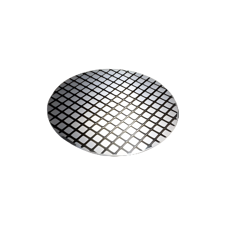
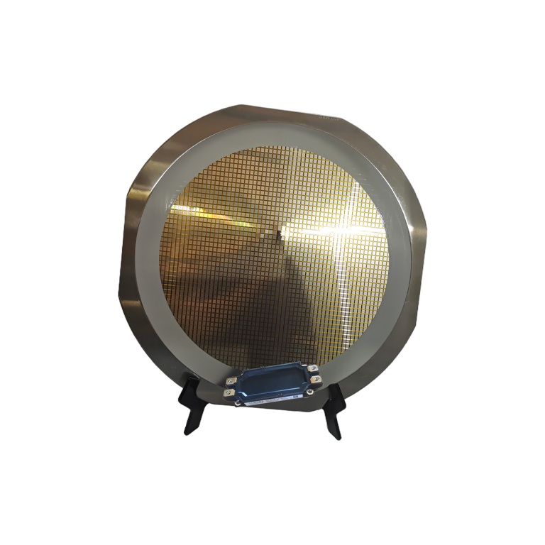
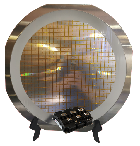
IGBT Wafer Construction Characteristics
IGBT wafers represent the fundamental semiconductor device in its most basic form, consisting of silicon substrate with processed junction layers but lacking any protective packaging or mounting infrastructure. These bare semiconductor devices require custom mounting solutions, wire bonding for electrical connections, and external thermal management systems designed specifically for each application.
The wafer construction provides maximum design flexibility since engineers can implement custom interconnection schemes, optimize thermal paths, and integrate the device directly into application-specific substrates. However, this flexibility comes with increased complexity in handling, mounting, and protecting the fragile semiconductor material from environmental factors and mechanical stress.
Engineers working with IGBT wafers must consider the semiconductor's delicate nature, requiring specialized assembly processes including die attachment, wire bonding, and encapsulation to create a functional power device suitable for industrial environments.
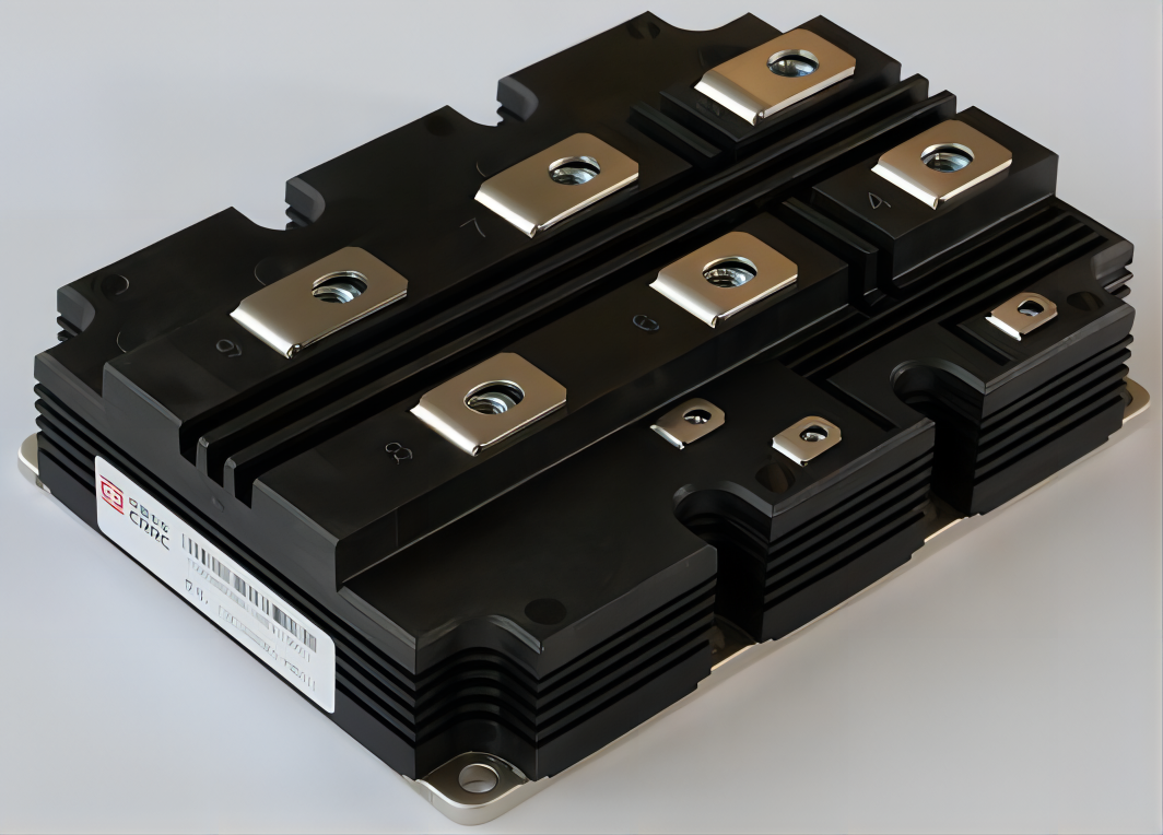
IGBT Module Integration and Protection
An IGBT module incorporates the semiconductor wafer within a complete package system that includes baseplate mounting, electrical terminals, thermal interface materials, and protective encapsulation. This integrated approach eliminates the need for custom assembly processes while providing standardized electrical and thermal interfaces.
The module construction typically features a direct bonded copper substrate that provides excellent thermal conductivity between the semiconductor junction and the mounting baseplate. Wire bond connections or advanced interconnection technologies like pressure contacts establish electrical connections within the protected environment of the module housing.
Modern IGBT Module designs incorporate advanced materials and construction techniques that optimize both electrical performance and thermal management while providing robust protection against environmental contamination, moisture, and mechanical vibration common in industrial applications.
Thermal Management and Heat Dissipation
Wafer-Level Thermal Considerations
IGBT wafers require custom thermal management solutions since they lack integrated heat spreading and mounting infrastructure. Engineers must design thermal paths that efficiently conduct heat from the small semiconductor junction area to larger heat sinking surfaces, often requiring specialized thermal interface materials and mounting techniques.
The thermal resistance characteristics of wafer implementations depend entirely on the custom thermal path design, making it possible to achieve very low junction-to-case thermal resistance values through optimized mounting and heat spreading techniques. However, achieving these optimal thermal characteristics requires careful engineering of the thermal stack-up and material selection.
Wafer-level implementations allow for direct liquid cooling approaches where coolant channels can be integrated very close to the semiconductor junction, potentially achieving superior thermal performance compared to conventional module approaches in specialized high-power applications.
Module Thermal Architecture Benefits
IGBT modules incorporate engineered thermal management systems that optimize heat transfer from the semiconductor junction through standardized thermal interfaces. The module construction typically includes direct bonded copper substrates that provide low thermal resistance paths combined with standardized mounting surfaces compatible with conventional heat sinks.
The integrated thermal design of an IGBT module eliminates thermal interface uncertainties while providing predictable thermal resistance specifications that engineers can use confidently in their thermal calculations. This standardization reduces design risk and accelerates development timelines compared to custom wafer implementations.
Advanced IGBT module designs incorporate features like integrated thermal monitoring, optimized heat spreading geometries, and specialized thermal interface materials that enhance heat dissipation performance while maintaining manufacturing consistency across production volumes.
Electrical Characteristics and Performance Parameters
Wafer Electrical Implementation Factors
IGBT wafers offer maximum flexibility in electrical interconnection design, allowing engineers to optimize wire bond layouts, minimize parasitic inductances, and implement custom gate drive interfaces tailored to specific switching requirements. This flexibility enables advanced electrical performance optimization but requires detailed electromagnetic modeling and custom interconnect design.
The electrical characteristics of wafer implementations depend heavily on the interconnection scheme, with factors like wire bond length, placement geometry, and substrate design significantly affecting switching performance, parasitic parameters, and electromagnetic compatibility characteristics.
Engineers implementing IGBT wafers must carefully consider current distribution uniformity across parallel devices, gate drive signal integrity, and electromagnetic field management to achieve optimal electrical performance while maintaining device reliability under high-frequency switching conditions.
Module Electrical Performance Standards
IGBT modules provide standardized electrical interfaces with characterized parasitic parameters, enabling predictable switching behavior and simplified gate drive circuit design. The module construction optimizes internal interconnections to minimize unwanted inductances and provide balanced current distribution across multi-chip configurations.
The electrical specifications of an IGBT module include comprehensive parametric data covering forward voltage drops, switching losses, gate charge requirements, and parasitic capacitances, allowing engineers to accurately model circuit behavior without extensive custom characterization efforts.
Module designs often incorporate features like integrated gate resistors, temperature sensing elements, and optimized current paths that enhance electrical performance while providing additional monitoring and protection capabilities essential for reliable power electronic system operation.
Application Suitability and Engineering Trade-offs
Wafer Implementation Advantages
IGBT wafers excel in applications requiring maximum power density, custom form factors, or specialized thermal management approaches where conventional module packaging would impose unacceptable constraints. Research applications, specialized aerospace systems, and ultra-high-power installations often benefit from wafer-level implementation flexibility.
The cost structure of wafer implementations can be advantageous in very high-volume applications where the engineering investment in custom assembly processes can be amortized across large production quantities. Additionally, wafers enable integration approaches that combine multiple functions within single custom packages.
Advanced applications requiring precise thermal management, minimal parasitic parameters, or integration with custom substrates and interconnection technologies often necessitate wafer-level implementations despite their increased engineering complexity and specialized manufacturing requirements.
Module Application Benefits
IGBT modules provide optimal solutions for mainstream industrial applications where standardized interfaces, proven reliability, and reduced engineering complexity outweigh the benefits of custom implementation. Motor drives, renewable energy systems, and industrial power supplies typically benefit from module-based approaches.
The reliability characteristics of IGBT modules include comprehensive qualification testing, standardized failure mode analysis, and predictable lifetime performance that supports industrial applications requiring extended operational periods with minimal maintenance requirements.
Module implementations enable faster time-to-market for power electronic systems by eliminating custom assembly processes, reducing design verification requirements, and providing access to comprehensive technical documentation and application support resources.
FAQ
What are the main cost differences between IGBT wafers and IGBT modules?
IGBT wafers typically have lower unit semiconductor costs but require significant additional expenses for custom assembly, packaging, qualification testing, and specialized manufacturing equipment. IGBT modules have higher unit costs but eliminate most custom assembly expenses and reduce overall system development costs for typical industrial applications. The total cost advantage depends on application volume, complexity requirements, and manufacturing capabilities.
How do reliability characteristics compare between wafer and module implementations?
IGBT modules generally provide superior reliability for standard applications due to their optimized packaging, comprehensive qualification testing, and proven manufacturing processes. Wafer implementations can achieve excellent reliability but require custom qualification programs and specialized assembly expertise. Module reliability is well-documented and predictable, while wafer reliability depends heavily on implementation quality and custom assembly processes.
Which approach offers better thermal performance for high-power applications?
IGBT wafers can potentially achieve superior thermal performance through custom thermal management solutions like direct liquid cooling and optimized heat spreading designs. However, IGBT modules provide excellent thermal performance with standardized interfaces that simplify thermal system design. For most applications, modules offer the best balance of thermal performance and engineering practicality, while wafers may be necessary for extreme thermal requirements.
When should engineers choose wafers over modules for new designs?
Engineers should consider IGBT wafers when applications require custom form factors that modules cannot accommodate, when maximum power density is critical, when specialized thermal management approaches are necessary, or when very high production volumes justify custom assembly investments. Most mainstream industrial applications benefit more from IGBT module implementations due to their reduced engineering complexity and proven reliability characteristics.
Table of Contents
- Physical Construction and Package Architecture
- Thermal Management and Heat Dissipation
- Electrical Characteristics and Performance Parameters
- Application Suitability and Engineering Trade-offs
-
FAQ
- What are the main cost differences between IGBT wafers and IGBT modules?
- How do reliability characteristics compare between wafer and module implementations?
- Which approach offers better thermal performance for high-power applications?
- When should engineers choose wafers over modules for new designs?