Brief introduction
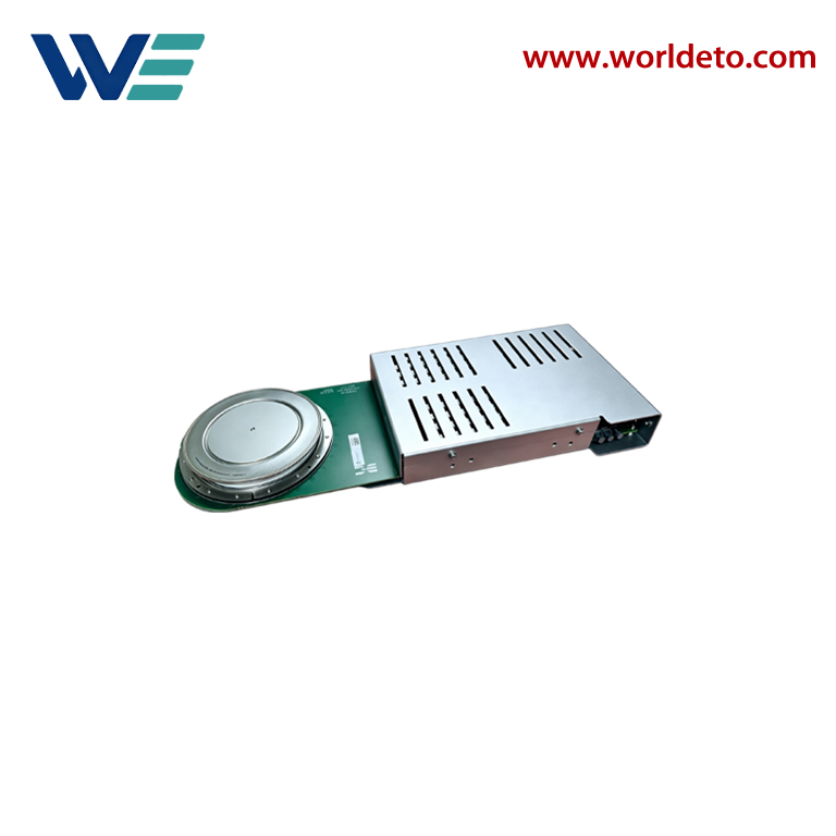
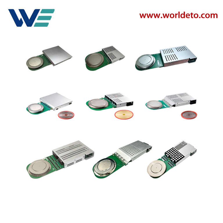
Asymmetric IGCT (A-IGCT) modules are high-power, high-reliability semiconductor devices designed for advanced medium- and high-voltage power conversion applications. By combining the high voltage and high current capability of GTO technology with the fast switching performance of IGCT technology, A-IGCT modules provide an efficient solution for demanding industrial power electronic systems.
Featuring advanced wafer manufacturing technology and optimized device structures, asymmetric IGCT modules offer low conduction losses, high turn-off capability, excellent thermal performance, and outstanding operational reliability. They are designed to ensure stable and long-term operation under harsh industrial conditions.
Asymmetric IGCT modules are widely used in high-voltage inverters, industrial rectifier power supplies, mining hoisting systems, railway traction, power quality improvement systems, large motor drives, and renewable energy power conversion systems.
Key Features:
High voltage capability for medium- and high-power applications
High current capability for large-scale power conversion systems
Low conduction losses for improved system efficiency
Fast turn-off performance for enhanced dynamic response
High reliability for continuous industrial operation
High power density design for compact power electronic systems
With excellent electrical performance and reliability, asymmetric IGCT modules provide a core semiconductor solution for next-generation high-efficiency and high-reliability power electronic systems.
YT-ASC40L6500IC
Key Parameters
V DRM |
6500 |
V |
I TGQM |
4000 |
A |
I TSM |
26 |
kA |
V TO |
1.88 |
V |
r T |
0.56 |
mQ |
V DClink |
4000 |
V |
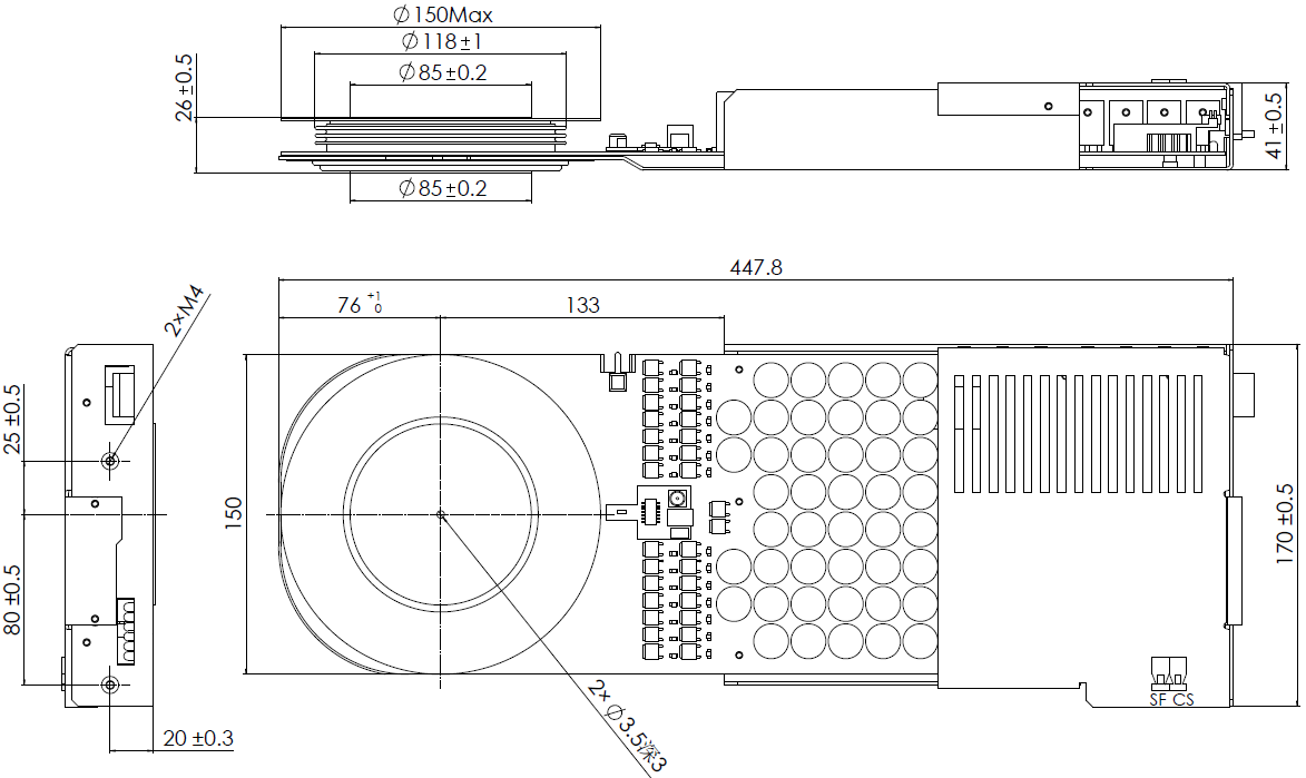
Mechanical Data
Symbol |
Parameter |
Conditions |
Min |
Typical |
Max |
|
V DRM |
Rep. peak off-state voltage |
T VJ=125℃, I D≤I DRM, t p=10ms |
- |
- |
4500 |
V |
I DRM |
Rep. peak off-state current |
T VJ=125℃, V D=V DRM, t p=10ms |
- |
- |
50 |
mA |
dv /dt |
Critical rate of rise of anode voltage |
T VJ=125℃, V D=0.67VDRM |
- |
- |
1000 |
V/μs |
V DClinK |
Intermediate DC voltage |
Permanent DC voltage for 100 FIT failure rate of GCT |
- |
- |
4000 |
V |
V RRM |
Reverse voltage |
\ |
- |
- |
17 |
V |
On-State Data
Symbol |
Parameter |
Conditions |
Min |
Typical |
Max |
|
I DC |
Max. RMS on-state current |
T C = 85℃, DC, Double side cooled |
- |
- |
2000 |
A |
|
I TSM
I 2 t
|
Max. peak non-repetitive surge on- state current
Limiting load integral
|
T VJ = 125℃, since half wave, 10ms,
V D=V R=0
|
-
-
|
-
-
|
26
338
|
KA
104A2 s
|
V TM |
On-state voltage |
T VJ = 125℃, I T =4000A |
- |
3.75 |
4.11 |
V |
|
V TO
r T
|
Threshold voltage
slope resistance
|
T VJ = 125℃, I T = 1000…4000A |
- |
- |
1.88
0.55
|
V
mΩ
|
Turn-on Data
Symbol |
Parameter name |
Test conditions |
Min |
Typical |
Max |
|
diT/dt |
Critical rate of rise of on-state current |
TVJ = 125℃, IT =4000A, VD = 2800V, f=0..500Hz |
- |
- |
5000 |
A/μs |
t don |
Turn-on delay time |
TVJ = 125℃, IT = 5000A, VD = 4000V,
di /dt = V D/Li , CCL =20μF, Li = 3μH, LCL = 0.3μH
|
- |
- |
3 |
μs |
t donSF |
Turn-on delay time status feedback |
- |
- |
7 |
μs |
t r |
Rise time (Fall time of anode voltage) |
- |
- |
1 |
μs |
Eon |
Turn-on energy per pulse |
- |
- |
3.3 |
J |
Turn-off Data
Symbol |
Parameter |
Conditions |
Min |
Typical |
Max |
|
ITGQM |
Max.controllable turn-off current |
T VJ = 125℃, V DM ≤ V DRM, V D =4000V, L CL = 0.3μH,
C CL = 20μF, R S = 0.4Ω,f=0..300Hz
DFWD = DCL= FYB 1100-60
|
- |
- |
4000 |
A |
tdoff |
Turn-off delay time |
T VJ = 125℃, I TGQ = 4000A, V D =4000V,
V DM ≤ V DRM, C CL = 20μF, R S = 0.4Ω,
L i =3μH, L CL = 0.3μH
DFWD = DCL= FYB 1100-60
|
- |
- |
8 |
μs |
tdoffSF |
Turn-off delay time status feedback |
- |
- |
7 |
μs |
tf |
Fall time |
- |
- |
1 |
μs |
Eoff |
Turn-off energy per pulse |
- |
442.5 |
46.3 |
J |
Thermal Data
Symbol |
Parameter name |
Test conditions |
Min |
Typical |
Max |
|
|
TVJ
TSTG
|
Junction operating temperature
Storage temperature range
|
/ |
0
-40
|
- |
125
60
|
℃
℃
|
|
RthJC
RthCH
|
Thermal resistance, junction-to-case
Thermal resistance, case-to-heatsink
|
Double side cooled |
-
-
|
-
-
|
8.5
3
|
K/kW
K/kW
|
Gate Unit
Symbol |
Parameter name |
Test conditions |
Min |
Typical |
Max |
|
V GIN RMS |
Gate unit voltage |
DC voltage or AC square wave amplitude (15kHz - 100kHz). No galvanic isolation to power circuit. |
28 |
- |
40 |
V |
P GIN MAX |
Max. Gate unit power consumption |
/ |
- |
- |
130 |
W |
I GIN MIN |
Min. Current needed to power up and
Gate Unit
|
Min. Current needed to power up and gate unit |
2 |
- |
- |
A |
I GIN MAX |
Internal current limitation |
Rectified average current limited by the
gate unit
|
- |
- |
8 |
A |
Optical Control input/output
|
t on(min)
t off(min)
|
Min. on- time
Min. off -time
|
/ |
40
40
|
-
-
|
-
-
|
μs
μs
|
|
P on CS
P Off CS
P on SF
P off SF
|
CS Optical input power
CS Optical noise power
SF Optical output power
SF Optical noise power
|
Valid for 1mm plastic optical fiber(POF) |
-15
-
-19
-
|
-
-
-
-
|
-1
-45
-1
-50
|
dBm
dBm
dBm
dBm
|
|
t GLITCH
t retrig
|
Pulse width threshold
External retrigger pulse width
|
Max. pulse width without response
/
|
-
700
|
-
-
|
400
1100
|
ns
ns
|
CS |
Receiver for command signal |
Agilent,Type:HFBR-2521 |
SF |
Transmitter for status feedback |
Agilent,Type:HFBR-1521 |
Visual Feedback
LED1(Green) |
Power Supply OK |
Light on when power supply is within specified range |
LED2(Green) |
Gate off |
Light on when GCT is off |
LED3(Yellow) |
Gate on |
Light on when gate-current is flowing |
LED4(Red) |
Fault |
Light on when gate drive capacitor is under voltage, or gate drive voltage is inconsistance with CS, or GCT is short circuited |
LED5(Yellow) |
TBD |
TBD |
LED6(Red) |
TBD |
TBD |

 EN
EN