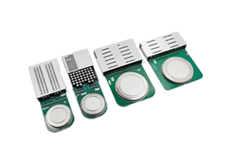
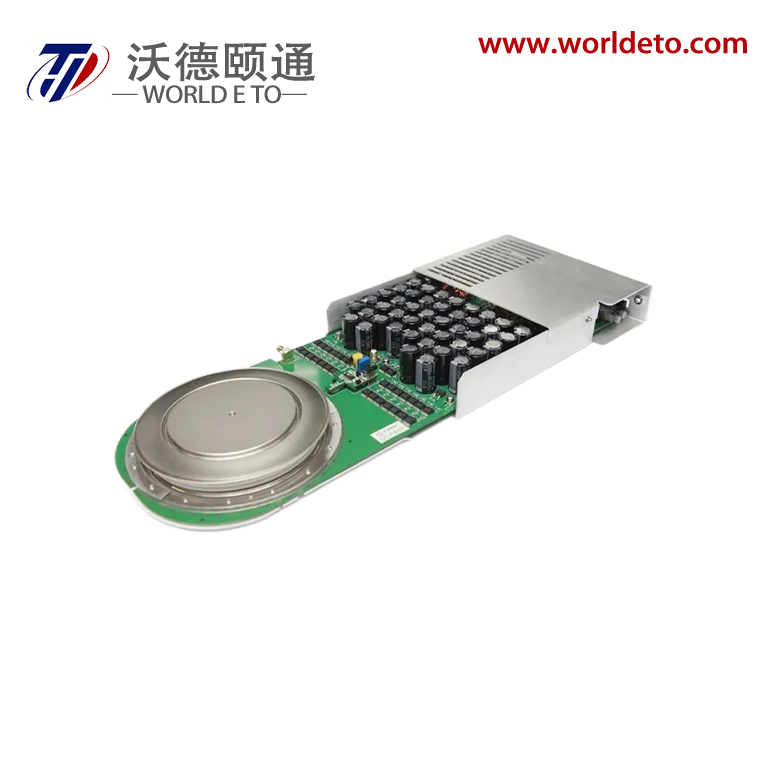
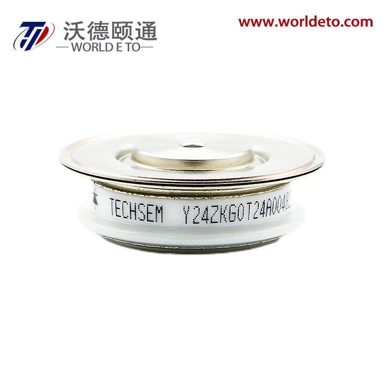
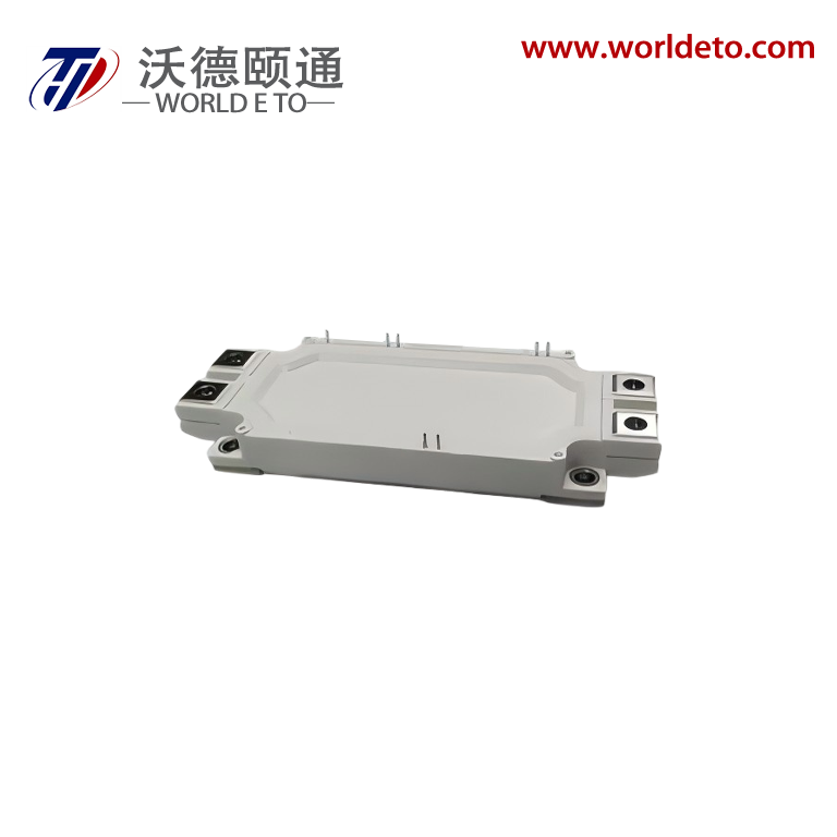
Brief introduction
IGCT module,Asymmetric Integrated Gate-Commutated Thyristor (IGCT) Plus,
produced by YT. 4500V 5000A.
Applications
- Modular multilevel converter
- Static var compensator
- High power converter
Features
- High withstand current
- Black-startup capability
- Failure short circuit mode
Key Parameters
V DRM |
4500 |
V |
I TGQM |
5000 |
A |
I T(RMS) |
3000 |
A |
I TSM |
35 |
kA |
V TO |
1.22 |
V |
r T |
0.28 |
mQ |
V DClink |
2800 |
V |
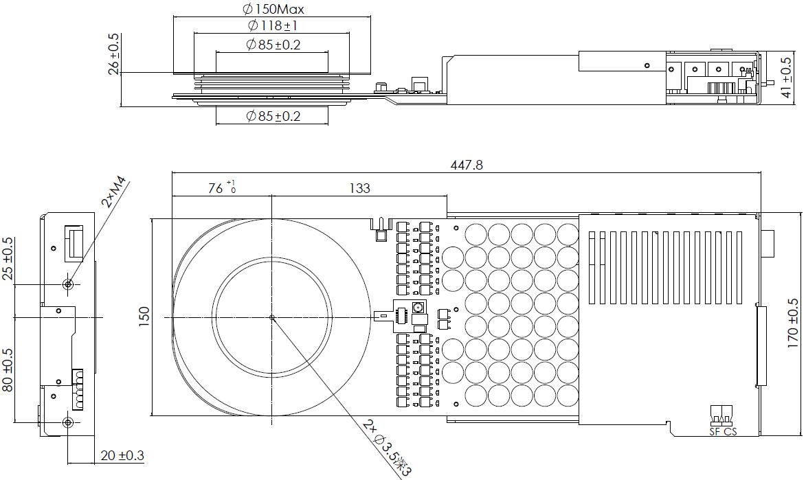
Mechanical Data
Symbol |
Parameter |
Min |
Typical |
Max |
|
F |
Mounting force |
36 |
40 |
44 |
kN |
Dp |
Pole-piece diamete |
- |
85 |
—— |
mm |
H |
Housing thickness |
- |
26 |
—— |
mm |
m |
weight |
- |
2.8 |
—— |
kg |
Ds |
Surface creepage |
33 |
- |
—— |
mm |
Da |
distance |
10 |
- |
—— |
mm |
L |
IGCT Length |
- |
447.8 |
—— |
mm |
H |
IGCT Height |
- |
41 |
|
mm |
W |
IGCT Width |
- |
170 |
|
mm |
Blocking Data
Symbol |
Parameter |
Conditions |
Min |
Typical |
Max |
|
V DRM |
Rep. peak off-state voltage |
T VJ=125℃, I D≤I DRM, t p=10ms |
- |
- |
4500 |
V |
I DRM |
Rep. peak off-state current |
T VJ=125℃, V D=V DRM, t p=10ms |
- |
- |
50 |
mA |
dv /dt |
Critical rate of rise of anode voltage |
T VJ=125℃, V D=0.67VDRM |
- |
- |
1000 |
V/μs |
V DClinK |
Permanent DC voltage for 100 FIT
failure rate of GCT
|
Allowable intermediate DC voltage of 100FIT failure rate |
- |
- |
2800 |
V |
V RRM |
Reverse voltage |
\ |
- |
- |
17 |
V |
On-State Data
Symbol |
Parameter |
Conditions |
Min |
Typical |
Max |
|
I T(RMS) |
Max. RMS on-state current |
T C = 85℃, Sin l half wave, double side cooling |
- |
- |
3000 |
A |
|
I TSM
I 2 t
|
Max. peak non-repetitive surge on-
state current
Limiting load integral
|
T VJ = 125℃, sin half wave, 10ms,
V D=V R=0
|
-
-
|
-
-
|
35
545
|
KA
104A2 s
|
V TM |
On-state voltage |
T VJ = 125℃, I T =5000A |
- |
2.37 |
2.61 |
V |
|
V TO
r T
|
Threshold voltage
slope resistance
|
T VJ = 125℃, I T = 1000…5000A |
- |
- |
1.22
0.28
|
V
mΩ
|
Turn-on Data
Symbol |
Parameter |
Conditions |
Min |
Typical |
Max |
|
diT/dt |
Critical rate of rise of on-state current |
TVJ = 125℃, IT = 5000A, VD = 2800V, f=0..500Hz |
- |
- |
5000 |
A/μs |
t don |
turn-on delay time |
TVJ = 125℃, IT = 5000A, VD = 2800V,
di /dt = V D/Li , CCL =20μF, RS =0.4Ω
Li = 3μH, LCL = 0.3μH
|
- |
- |
4 |
μs |
t donSF |
Turn-on delay time status feedback |
- |
- |
7 |
μs |
t r |
Rise time (Fall time of anode voltage) |
- |
- |
1 |
μs |
Eon |
Turn-on energy per pulse |
- |
- |
1.8 |
J |
Turn-off Data
Symbol |
Parameter name |
Test conditions |
Min |
Typical |
Max |
|
ITGQM |
Max.controllable turn-off current |
TVJ = 125℃, VDM ≤V DRM, V D =2800V,
L CL = 0.3μH, C CL = 20μF, R S = 0.4Ω,
f=0..300Hz
DFWD = DCL=SF8.FYB2000-45
|
- |
- |
5000 |
A |
tdoff |
Surn-off delay time |
T VJ = 125℃, I TGQ = 5000A, V D =2800V,
V DM ≤ V DRM, C CL = 20μF, R S = 0.4Ω,
L i =4μH, L CL = 0.3μH
DFWD = DCL= SF8.FYB2000-45
|
- |
- |
8 |
μs |
tdoffSF |
Turn-off delay time status
feedback
|
- |
- |
7 |
μs |
tf |
Fall time |
- |
- |
1 |
μs |
Eoff |
Turn-off energy per pulse |
- |
28 |
33 |
J |
Thermal Data
Symbol |
Parameter |
Conditions |
Min |
Typical |
Max |
|
|
TVJ
TSTG
|
Junction operating temperature
Storage temperature range
|
/ |
0
-40
|
- |
125
60
|
℃
℃
|
|
RthJC
RthCH
|
Thermal resistance, junction-to- Case
Thermal resistance, case-to- heatsink
|
Double sided cooling |
-
-
|
-
-
|
8.5
3
|
K/kW
K/kW
|
Gate Unit
Symbol |
Parameter |
Conditions |
Min |
Typical |
Max |
|
V GIN RMS |
Gate unit voltage |
DC voltage or AC square wave amplitude (15kHz -
100kHz). No galvanic isolation to power circuit.
|
28 |
- |
40 |
V |
P GIN MAX |
Max. Gate unit power consumption |
/ |
- |
- |
130 |
W |
I GIN MIN |
Min. Current needed to power up and Gate Unit |
Min. Current needed to power up and gate unit |
2 |
- |
- |
A |
I GIN MAX |
Internal current limitation |
Rectified average current limited by the gate unit |
- |
- |
8 |
A |
Optical Control input/output
|
t on(min)
t off(min)
|
Min on- time
Min off -time
|
/ |
40
40
|
-
-
|
-
-
|
μs
μs
|
|
P on CS
P Off CS
P on SF
P off SF
|
CS Optical input power
CS Optical noise power
SF Optical output power
SF Optical noise power
|
Valid for 1mm plastic optical fiber(POF) |
-15
-
-19
-
|
-
-
-
-
|
-1
-45
-1
-50
|
dBm
dBm
dBm
dBm
|
|
t GLITCH
t retrig
|
Pulse width threshold
External retrigger pulse width
|
Max. pulse width without response
/
|
-
700
|
-
-
|
400
1100
|
ns
ns
|
CS |
Receiver for command signal |
Agilent,Type:HFBR-2521 |
SF |
Transmitter for status feedback |
Agilent,Type:HFBR-1521 |
Visual Feedback
LED1(Green) |
Power Supply OK |
Light on when power supply is within specified range |
LED2(Green) |
Gate off |
Light on when GCT is off |
LED3(Yellow) |
Gate on |
Light on when gate-current is flowing |
LED4(Red) |
Fault |
Light on when gate drive capacitor is under voltage, or gate drive voltage is inconsistance with CS, or GCT is short circuited |
LED5(Yellow) |
TBD |
TBD |
LED6(Red) |
TBD |
TBD |