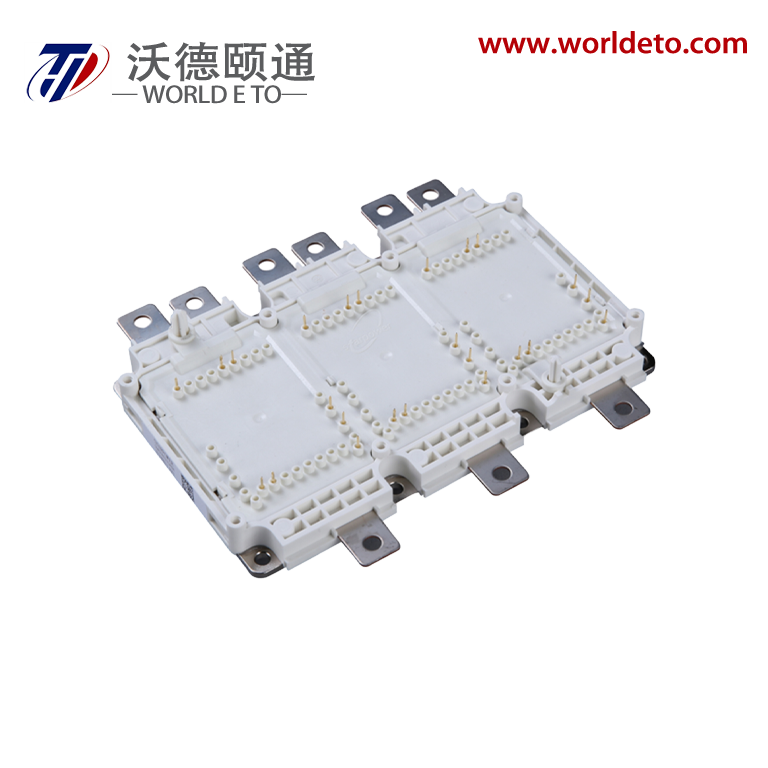
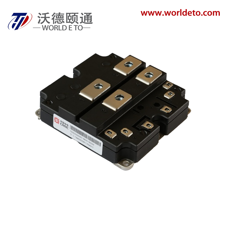
Brief introduction
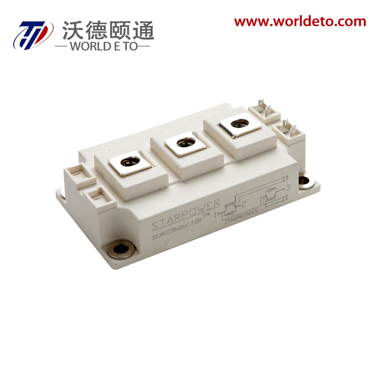
IGBT module,produced by STARPOWER. 1000V 750A.
Features
- Low VCE(sat) Trench IGBT technology
- Low switching losses
- 6μs short circuit capability
- VCE(sat) with positive temperature coefficient
-
Maximum junction temperature 175℃
- Low inductance case
- Fast & soft reverse recovery anti-parallel FWD
-
Isolated copper pinfin baseplate using Si3N4 AMB technology
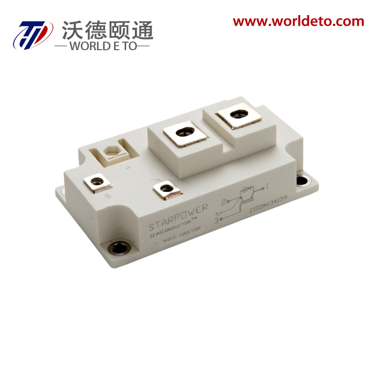
Typical Applications
- Automotive application
- Hybrid and electric vehicle
- Inverter for motor drive
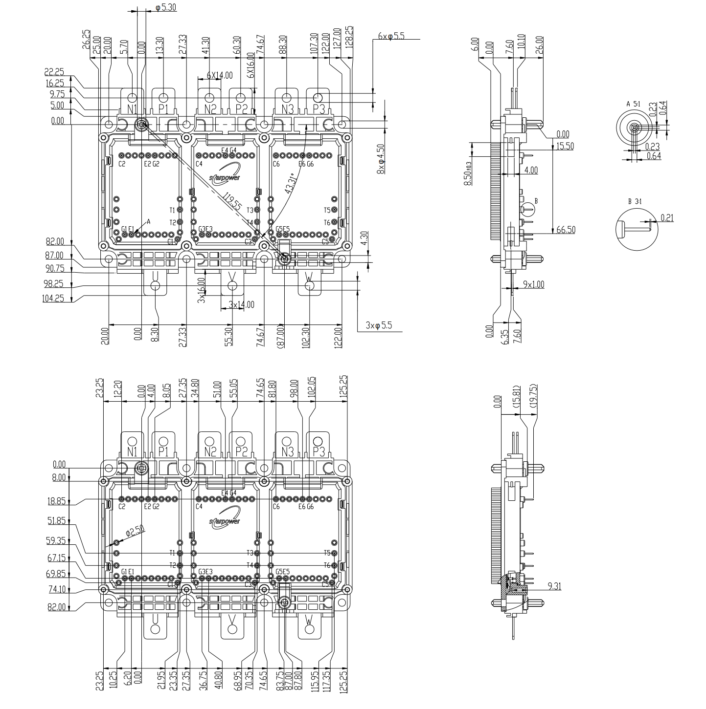
Absolute Maximum Ratings TF=25oC unless otherwise noted
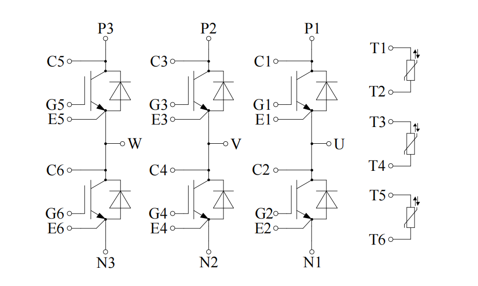
IGBT
Symbol |
Description |
Values |
Unit |
VCES |
Collector-Emitter Voltage |
750 |
V |
VGES |
Gate-Emitter Voltage |
±20 |
V |
ICN |
Implemented Collector Current |
1000 |
A |
IC |
Collector Current @ TF=125oC |
450 |
A |
ICM |
Pulsed Collector Current tp=1ms |
2000 |
A |
PD |
Maximum Power Dissipation @ TF=75oC Tvj=175oC |
1282 |
W |
Diode
Symbol |
Description |
Values |
Unit |
VRRM |
Repetitive Peak Reverse Voltage |
750 |
V |
IFN |
Implemented Collector Current |
1000 |
A |
IF |
Diode Continuous Forward Current |
450 |
A |
IFM |
Diode Maximum Forward Current tp=1ms |
2000 |
A |
Module
Symbol |
Description |
Value |
Unit |
Tvjmax |
Maximum Junction Temperature |
175 |
oC |
Tvjop |
Operating Junction Temperature continuous
For 10s within a period of 30s,occurrence maximum 3000 times over lifetime
|
-40 to +150 +150 to +175 |
oC |
TSTG |
Storage Temperature Range |
-40 to +125 |
oC |
VISO |
Isolation Voltage RMS,f=50Hz,t=1min |
2500 |
V |
dCreep |
Terminal to Heatsink Terminal to Terminal |
9.0 9.0 |
mm |
dClear |
Terminal to Heatsink Terminal to Terminal |
4.5 4.5 |
mm |
IGBT Characteristics TF=25oC unless otherwise noted
Symbol |
Parameter |
Test Conditions |
Min. |
Typ. |
Max. |
Unit |
|
|
VCE(sat)
|
Collector to Emitter Saturation Voltage
|
IC=450A,VGE=15V, Tvj=25oC |
|
1.10 |
1.35 |
V
|
|
IC=450A,VGE=15V, Tvj=150oC |
|
1.10 |
|
|
IC=450A,VGE=15V, Tvj=175oC |
|
1.10 |
|
|
IC=1000A,VGE=15V, Tvj=25oC |
|
1.40 |
|
|
IC=1000A,VGE=15V, Tvj=175oC |
|
1.60 |
|
|
VGE(th) |
Gate-Emitter Threshold Voltage |
IC=12.9mA,VCE=VGE, Tvj=25oC |
5.5 |
6.4 |
7.0 |
V |
|
ICES |
Collector Cut-Off Current |
VCE=VCES,VGE=0V, Tvj=25oC |
|
|
1.0 |
mA |
|
IGES |
Gate-Emitter Leakage Current |
VGE=VGES,VCE=0V, Tvj=25oC |
|
|
400 |
nA |
|
RGint |
Internal Gate Resistance |
|
|
1.2 |
|
Ω |
|
Cies |
Input Capacitance |
VCE=50V,f=100kHz, VGE=0V
|
|
66.7 |
|
nF |
|
Coes |
Output Capacitance |
|
1.50 |
|
nF |
|
Cres |
Reverse Transfer Capacitance |
|
0.35 |
|
nF |
|
QG |
Gate Charge |
VCE =400V,IC =450A, VGE=-15…+15V |
|
4.74 |
|
μC |
|
td(on) |
Turn-On Delay Time |
VCC=400V,IC=450A,
RGon=1.2Ω,RGoff=1.0Ω, VGE=-8V/+15V,
LS=24nH, Tvj=25oC
|
|
244 |
|
ns |
|
tr |
Rise Time |
|
61 |
|
ns |
|
td(off) |
Turn-Off Delay Time |
|
557 |
|
ns |
|
tf |
Fall Time |
|
133 |
|
ns |
|
Eon |
Turn-On Switching Loss |
|
11.0 |
|
mJ |
|
Eoff |
Turn-Off Switching Loss |
|
22.8 |
|
mJ |
|
td(on) |
Turn-On Delay Time |
VCC=400V,IC=450A,
RGon=1.2Ω,RGoff=1.0Ω, VGE=-8V/+15V,
LS=24nH, Tvj=150oC
|
|
260 |
|
ns |
|
tr |
Rise Time |
|
68 |
|
ns |
|
td(off) |
Turn-Off Delay Time |
|
636 |
|
ns |
|
tf |
Fall Time |
|
226 |
|
ns |
|
Eon |
Turn-On Switching Loss |
|
16.9 |
|
mJ |
|
Eoff |
Turn-Off Switching Loss |
|
32.2 |
|
mJ |
|
td(on) |
Turn-On Delay Time |
VCC=400V,IC=450A,
RGon=1.2Ω,RGoff=1.0Ω, VGE=-8V/+15V,
LS=24nH, Tvj=175oC
|
|
264 |
|
ns |
|
tr |
Rise Time |
|
70 |
|
ns |
|
td(off) |
Turn-Off Delay Time |
|
673 |
|
ns |
|
tf |
Fall Time |
|
239 |
|
ns |
|
Eon |
Turn-On Switching Loss |
|
19.2 |
|
mJ |
|
Eoff |
Turn-Off Switching Loss |
|
33.6 |
|
mJ |
|
ISC |
SC Data |
tP≤6μs,VGE=15V,
Tvj=25oC,VCC=400V, VCEM≤750V
|
|
4900 |
|
A |
|
|
|
tP≤3μs,VGE=15V,
Tvj=175oC,VCC=400V, VCEM≤750V
|
|
3800
|
|
|
|
Diode Characteristics TF=25oC unless otherwise noted
Symbol |
Parameter |
Test Conditions |
Min. |
Typ. |
Max. |
Unit |
|
VF
|
Diode Forward Voltage
|
IF=450A,VGE=0V,Tvj=25oC |
|
1.40 |
1.65 |
V
|
IF=450A,VGE=0V,Tvj=150oC |
|
1.35 |
|
IF=450A,VGE=0V,Tvj=175oC |
|
1.30 |
|
IF=1000A,VGE=0V,Tvj=25oC |
|
1.80 |
|
IF=1000A,VGE=0V,Tvj=175oC |
|
1.80 |
|
Qr |
Recovered Charge |
VR=400V,IF=450A,
-di/dt=7809A/μs,VGE=-8V LS=24nH,Tvj=25oC
|
|
18.5 |
|
μC |
IRM |
Peak Reverse
Recovery Current
|
|
303 |
|
A |
Erec |
Reverse Recovery Energy |
|
3.72 |
|
mJ |
Qr |
Recovered Charge |
VR=400V,IF=450A,
-di/dt=6940A/μs,VGE=-8V LS=24nH,Tvj=150oC
|
|
36.1 |
|
μC |
IRM |
Peak Reverse
Recovery Current
|
|
376 |
|
A |
Erec |
Reverse Recovery Energy |
|
8.09 |
|
mJ |
Qr |
Recovered Charge |
VR=400V,IF=450A,
-di/dt=6748A/μs,VGE=-8V LS=24nH,Tvj=175oC
|
|
40.1 |
|
μC |
IRM |
Peak Reverse
Recovery Current
|
|
383 |
|
A |
Erec |
Reverse Recovery Energy |
|
9.01 |
|
mJ |
NTC Characteristics TF=25oC unless otherwise noted
Symbol |
Parameter |
Test Conditions |
Min. |
Typ. |
Max. |
Unit |
R25 |
Rated Resistance |
|
|
5.0 |
|
kΩ |
∆R/R |
Deviation of R100 |
TC=100 oC,R100=493.3Ω |
-5 |
|
5 |
% |
P25 |
Power
Dissipation
|
|
|
|
20.0 |
mW |
B25/50 |
B-value |
R2=R25exp[B25/50(1/T2- 1/(298.15K))] |
|
3375 |
|
K |
B25/80 |
B-value |
R2=R25exp[B25/80(1/T2- 1/(298.15K))] |
|
3411 |
|
K |
B25/100 |
B-value |
R2=R25exp[B25/100(1/T2- 1/(298.15K))] |
|
3433 |
|
K |
Module Characteristics TF=25oC unless otherwise noted
Symbol |
Parameter |
Min. |
Typ. |
Max. |
Unit |
LCE |
Stray Inductance |
|
8 |
|
nH |
RCC’+EE’ |
Module Lead Resistance, Terminal to Chip |
|
0.75 |
|
mΩ |
|
p
|
Maximum Pressure In Cooling Circuit
Tbaseplate<40oC
Tbaseplate 40oC
(relative pressure)
|
|
|
2.5 2.0 |
bar
|
|
RthJF
|
Junction-to-Cooling Fluid (perIGBT) Junction-to-Cooling Fluid (per Diode) △V/△t=10.0dm3/min,TF=75oC |
|
0.068 0.105 |
0.078 0.120 |
K/W |
M |
Terminal Connection Torque, Screw M5 Mounting Torque, Screw M4 |
3.6 1.8 |
|
4.4 2.2 |
N.m |
G |
Weight of Module |
|
750 |
|
g |