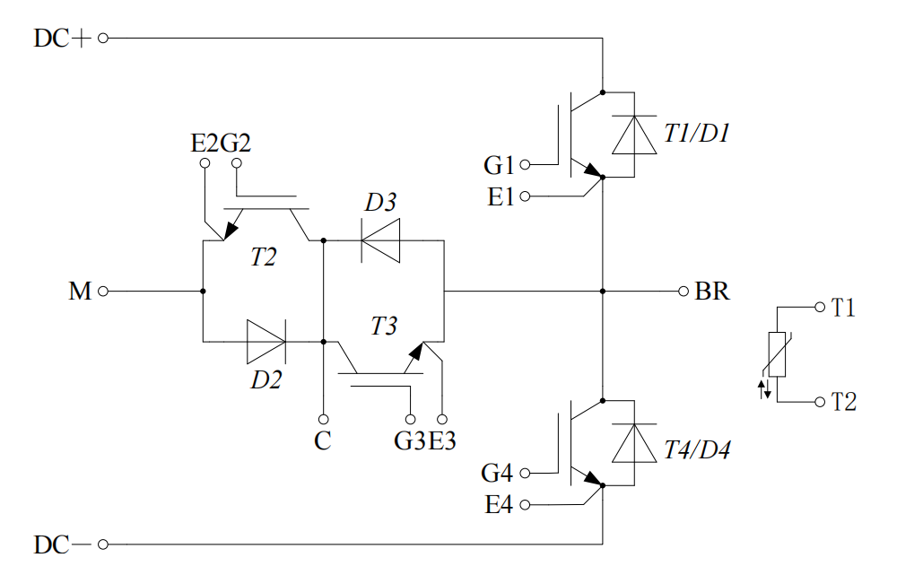
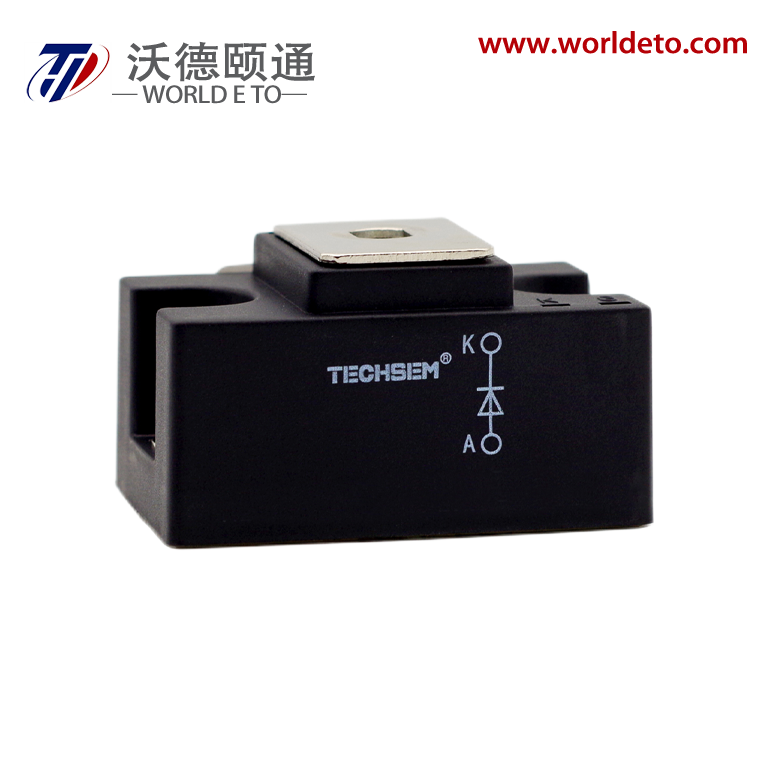
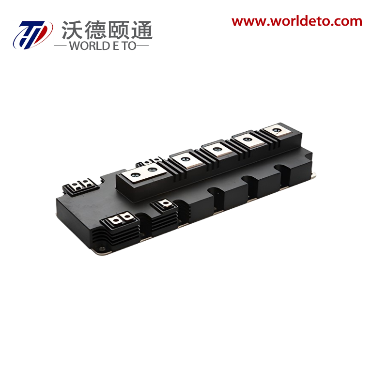
Brief introduction
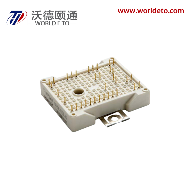
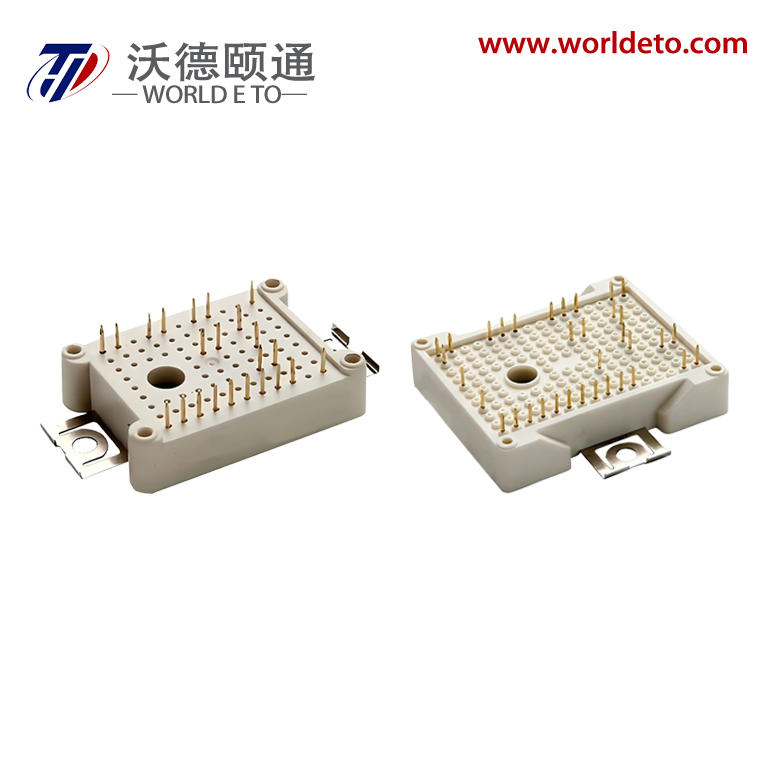
IGBT module, produced by STARPOWER. 1200V 200A.
Features
- Low VCE(sat) Trench IGBT technology
- Low switching loss
- Short circuit capability
- VCE(sat) with positive temperature coefficient
- Maximum junction temperature 175oC
- Fast & soft reverse recovery anti-parallel FWD
- Low inductance case
- Isolated heatsink using DBC technology
Typical Applications
Absolute Maximum Ratings TC=25oC unless otherwise noted
T1,T4 IGBT
Symbol |
Description |
Values |
Unit |
VCES |
Collector-Emitter Voltage |
1200 |
V |
VGES |
Gate-Emitter Voltage |
±20 |
V |
IC |
Collector Current @ TC=25oC
@ TC= 100oC
|
339
200
|
A |
ICM |
Pulsed Collector Current tp= 1ms |
400 |
A |
PD |
Maximum Power Dissipation @ Tj=175oC |
1456 |
W |
D1,D4 Diode
Symbol |
Description |
Value |
Unit |
VRRM |
Repetitive Peak Reverse Voltage |
1200 |
V |
IF |
Diode Continuous Forward Current |
75 |
A |
IFM |
Diode Maximum Forward Current tp= 1ms |
150 |
A |
T2,T3 IGBT
Symbol |
Description |
Value |
Unit |
VCES |
Collector-Emitter Voltage |
650 |
V |
VGES |
Gate-Emitter Voltage |
±20 |
V |
IC |
Collector Current @ TC=25oC
@ TC=95oC
|
158
100
|
A |
ICM |
Pulsed Collector Current tp= 1ms |
200 |
A |
PD |
Maximum Power Dissipation @ Tj=175oC |
441 |
W |
D2,D3 Diode
Symbol |
Description |
Value |
Unit |
VRRM |
Repetitive Peak Reverse Voltage |
650 |
V |
IF |
Diode Continuous Forward Current |
100 |
A |
IFM |
Diode Maximum Forward Current tp= 1ms |
200 |
A |
Module
Symbol |
Description |
Value |
Unit |
Tjmax |
Maximum Junction Temperature |
175 |
oC |
Tjop |
Operating Junction Temperature |
-40 to +150 |
oC |
TSTG |
Storage Temperature Range |
-40 to +125 |
oC |
VISO |
Isolation Voltage RMS,f=50Hz,t=1min |
2500 |
V |
T1,T4 IGBT Characteristics TC=25oC unless otherwise noted
Symbol |
Parameter |
Test Conditions |
Min. |
Typ. |
Max. |
Unit |
|
VCE(sat)
|
Collector to Emitter
Saturation Voltage
|
IC= 100A,VGE= 15V, Tj=25oC |
|
1.40 |
1.85 |
V
|
IC= 100A,VGE= 15V, Tj=125oC |
|
1.65 |
|
IC= 100A,VGE= 15V, Tj=150oC |
|
1.70 |
|
VGE(th) |
Gate-Emitter Threshold Voltage |
IC=5.0mA,VCE=VGE, Tj=25oC |
5.2 |
6.0 |
6.8 |
V |
ICES |
Collector Cut-Off
Current
|
VCE=VCES,VGE=0V,
Tj=25oC
|
|
|
1.0 |
mA |
IGES |
Gate-Emitter Leakage Current |
VGE=VGES,VCE=0V, Tj=25oC |
|
|
400 |
nA |
RGint |
Internal Gate Resistance |
|
|
3.8 |
|
Ω |
Cies |
Input Capacitance |
VCE=25V,f=1MHz,
VGE=0V
|
|
20.7 |
|
nF |
Cres |
Reverse Transfer
Capacitance
|
|
0.58 |
|
nF |
QG |
Gate Charge |
VGE=- 15…+15V |
|
1.56 |
|
μC |
td(on) |
Turn-On Delay Time |
VCC=400V,IC= 100A, RG= 1. 1Ω,VGE=±15V, Tj=25oC
|
|
142 |
|
ns |
tr |
Rise Time |
|
25 |
|
ns |
td(off) |
Turn-Off Delay Time |
|
352 |
|
ns |
tf |
Fall Time |
|
33 |
|
ns |
Eon |
Turn-On Switching
Loss
|
|
1.21 |
|
mJ |
Eoff |
Turn-Off Switching
Loss
|
|
3.90 |
|
mJ |
td(on) |
Turn-On Delay Time |
VCC=400V,IC= 100A, RG= 1. 1Ω,VGE=±15V, Tj= 125oC
|
|
155 |
|
ns |
tr |
Rise Time |
|
29 |
|
ns |
td(off) |
Turn-Off Delay Time |
|
440 |
|
ns |
tf |
Fall Time |
|
61 |
|
ns |
Eon |
Turn-On Switching
Loss
|
|
2.02 |
|
mJ |
Eoff |
Turn-Off Switching
Loss
|
|
5.83 |
|
mJ |
td(on) |
Turn-On Delay Time |
VCC=400V,IC= 100A, RG= 1. 1Ω,VGE=±15V, Tj= 150oC
|
|
161 |
|
ns |
tr |
Rise Time |
|
30 |
|
ns |
td(off) |
Turn-Off Delay Time |
|
462 |
|
ns |
tf |
Fall Time |
|
66 |
|
ns |
Eon |
Turn-On Switching
Loss
|
|
2.24 |
|
mJ |
Eoff |
Turn-Off Switching
Loss
|
|
6.49 |
|
mJ |
|
ISC
|
SC Data
|
tP≤10μs,VGE=15V,
Tj=150oC,VCC=800V, VCEM≤1200V
|
|
800
|
|
A
|
D1,D4 Diode Characteristics TC=25oC unless otherwise noted
Symbol |
Parameter |
Test Conditions |
Min. |
Typ. |
Max. |
Unit |
|
VF
|
Diode Forward
Voltage
|
IF=75A,VGE=0V,Tj=25oC |
|
1.70 |
2.15 |
V
|
IF=75A,VGE=0V,Tj= 125oC |
|
1.65 |
|
IF=75A,VGE=0V,Tj= 150oC |
|
1.65 |
|
Qr |
Recovered Charge |
VR=400V,IF=75A,
-di/dt=3500A/μs,VGE=- 15V Tj=25oC
|
|
8.7 |
|
μC |
IRM |
Peak Reverse
Recovery Current
|
|
122 |
|
A |
Erec |
Reverse Recovery Energy |
|
2.91 |
|
mJ |
Qr |
Recovered Charge |
VR=400V,IF=75A,
-di/dt=3500A/μs,VGE=- 15V Tj= 125oC
|
|
17.2 |
|
μC |
IRM |
Peak Reverse
Recovery Current
|
|
143 |
|
A |
Erec |
Reverse Recovery Energy |
|
5.72 |
|
mJ |
Qr |
Recovered Charge |
VR=400V,IF=75A,
-di/dt=3500A/μs,VGE=- 15V Tj= 150oC
|
|
19.4 |
|
μC |
IRM |
Peak Reverse
Recovery Current
|
|
152 |
|
A |
Erec |
Reverse Recovery Energy |
|
6.30 |
|
mJ |
T2,T3 IGBT Characteristics TC=25oC unless otherwise noted
Symbol |
Parameter |
Test Conditions |
Min. |
Typ. |
Max. |
Unit |
|
VCE(sat)
|
Collector to Emitter
Saturation Voltage
|
IC= 100A,VGE= 15V, Tj=25oC |
|
1.45 |
1.90 |
V
|
IC= 100A,VGE= 15V, Tj=125oC |
|
1.60 |
|
IC= 100A,VGE= 15V, Tj=150oC |
|
1.70 |
|
VGE(th) |
Gate-Emitter Threshold Voltage |
IC= 1.60mA,VCE=VGE, Tj=25oC |
5.0 |
5.8 |
6.5 |
V |
ICES |
Collector Cut-Off
Current
|
VCE=VCES,VGE=0V,
Tj=25oC
|
|
|
1.0 |
mA |
IGES |
Gate-Emitter Leakage Current |
VGE=VGES,VCE=0V, Tj=25oC |
|
|
400 |
nA |
RGint |
Internal Gate Resistance |
|
|
2.0 |
|
Ω |
Cies |
Input Capacitance |
VCE=25V,f=1MHz,
VGE=0V
|
|
11.6 |
|
nF |
Cres |
Reverse Transfer
Capacitance
|
|
0.23 |
|
nF |
QG |
Gate Charge |
VGE=- 15…+15V |
|
0.69 |
|
μC |
td(on) |
Turn-On Delay Time |
VCC=400V,IC= 100A, RG=3.3Ω,VGE=±15V, Tj=25oC
|
|
44 |
|
ns |
tr |
Rise Time |
|
20 |
|
ns |
td(off) |
Turn-Off Delay Time |
|
200 |
|
ns |
tf |
Fall Time |
|
28 |
|
ns |
Eon |
Turn-On Switching
Loss
|
|
1.48 |
|
mJ |
Eoff |
Turn-Off Switching
Loss
|
|
2.48 |
|
mJ |
td(on) |
Turn-On Delay Time |
VCC=400V,IC= 100A, RG=3.3Ω,VGE=±15V, Tj= 125oC
|
|
48 |
|
ns |
tr |
Rise Time |
|
24 |
|
ns |
td(off) |
Turn-Off Delay Time |
|
216 |
|
ns |
tf |
Fall Time |
|
40 |
|
ns |
Eon |
Turn-On Switching
Loss
|
|
2.24 |
|
mJ |
Eoff |
Turn-Off Switching
Loss
|
|
3.28 |
|
mJ |
td(on) |
Turn-On Delay Time |
VCC=400V,IC= 100A, RG=3.3Ω,VGE=±15V, Tj= 150oC
|
|
52 |
|
ns |
tr |
Rise Time |
|
24 |
|
ns |
td(off) |
Turn-Off Delay Time |
|
224 |
|
ns |
tf |
Fall Time |
|
48 |
|
ns |
Eon |
Turn-On Switching
Loss
|
|
2.64 |
|
mJ |
Eoff |
Turn-Off Switching
Loss
|
|
3.68 |
|
mJ |
|
ISC
|
SC Data
|
tP≤6μs,VGE= 15V,
Tj=150oC,VCC=360V, VCEM≤650V
|
|
500
|
|
A
|
D2,D3 Diode Characteristics TC=25oC unless otherwise noted
Symbol |
Parameter |
Test Conditions |
Min. |
Typ. |
Max. |
Unit |
|
VF
|
Diode Forward
Voltage
|
IF= 100A,VGE=0V,Tj=25oC |
|
1.55 |
2.00 |
V
|
IF= 100A,VGE=0V,Tj= 125oC |
|
1.50 |
|
IF= 100A,VGE=0V,Tj= 150oC |
|
1.45 |
|
Qr |
Recovered Charge |
VR=400V,IF= 100A,
-di/dt=4070A/μs,VGE=- 15V Tj=25oC
|
|
3.57 |
|
μC |
IRM |
Peak Reverse
Recovery Current
|
|
99 |
|
A |
Erec |
Reverse Recovery Energy |
|
1.04 |
|
mJ |
Qr |
Recovered Charge |
VR=400V,IF= 100A,
-di/dt=4070A/μs,VGE=- 15V Tj= 125oC
|
|
6.49 |
|
μC |
IRM |
Peak Reverse
Recovery Current
|
|
110 |
|
A |
Erec |
Reverse Recovery Energy |
|
1.70 |
|
mJ |
Qr |
Recovered Charge |
VR=400V,IF= 100A,
-di/dt=4070A/μs,VGE=- 15V Tj= 150oC
|
|
7.04 |
|
μC |
IRM |
Peak Reverse
Recovery Current
|
|
110 |
|
A |
Erec |
Reverse Recovery Energy |
|
1.81 |
|
mJ |
NTC Characteristics TC=25oC unless otherwise noted
Symbol |
Parameter |
Test Conditions |
Min. |
Typ. |
Max. |
Unit |
R25 |
Rated Resistance |
|
|
5.0 |
|
kΩ |
ΔR/R |
Deviation of R100 |
TC= 100 oC,R100=493.3Ω |
-5 |
|
5 |
% |
P25 |
Power
Dissipation
|
|
|
|
20.0 |
mW |
B25/50 |
B-value |
R2=R25exp[B25/50(1/T2-
1/(298.15K))]
|
|
3375 |
|
K |
B25/80 |
B-value |
R2=R25exp[B25/80(1/T2-
1/(298.15K))]
|
|
3411 |
|
K |
B25/100 |
B-value |
R2=R25exp[B25/100(1/T2-
1/(298.15K))]
|
|
3433 |
|
K |
Module Characteristics TC=25oC unless otherwise noted
Symbol |
Parameter |
Min. |
Typ. |
Max. |
Unit |
|
RthJC
|
Junction-to-Case (per T1,T4 IGBT)
Junction-to-Case (per D1,D4 Diode)
Junction-to-Case (per T2,T3 IGBT)
Junction-to-Case (per D2,D3 Diode)
|
|
0.094
0.405
0.309
0.544
|
0.103
0.446
0.340
0.598
|
K/W
|
|
RthCH
|
Case-to-Heatsink (per T1,T4 IGBT)
Case-to-Heatsink (per D1,D4 Diode)
Case-to-Heatsink (per T2,T3 IGBT)
Case-to-Heatsink (per D2,D3 Diode)
Case-to-Heatsink (per Module)
|
|
0.126
0.547
0.417
0.733
0.037
|
|
K/W
|
F |
Mounting Force Per Clamp |
40 |
|
80 |
N |
G |
Weight of Module |
|
39 |
|
g |