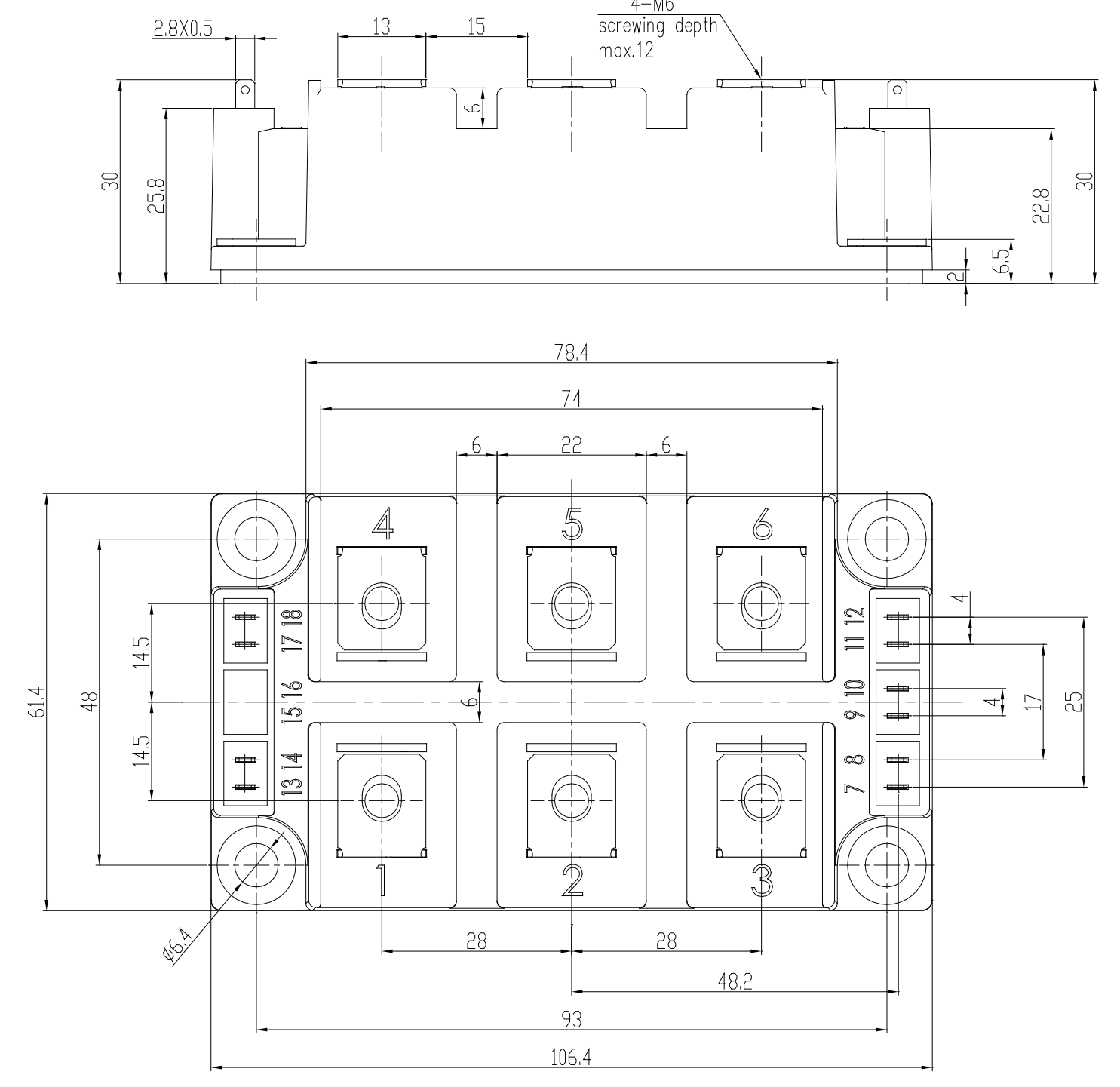
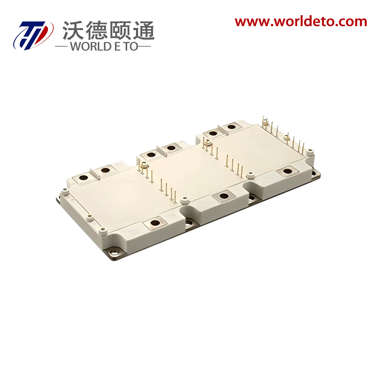
Brief introduction
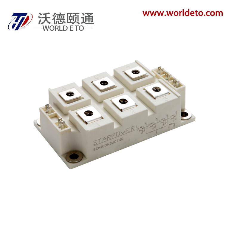
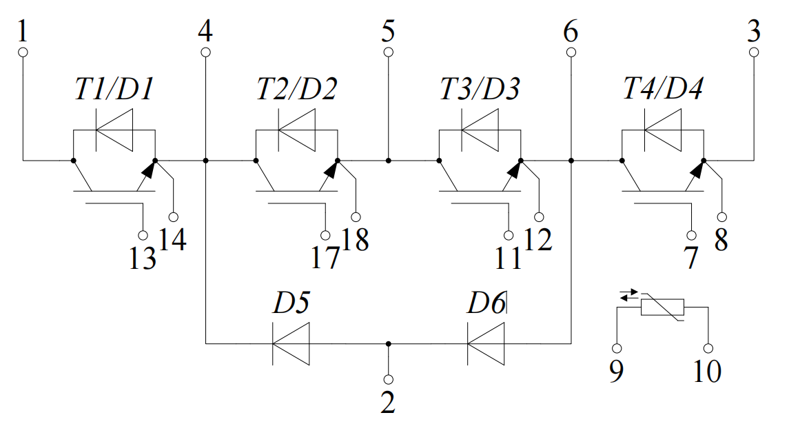
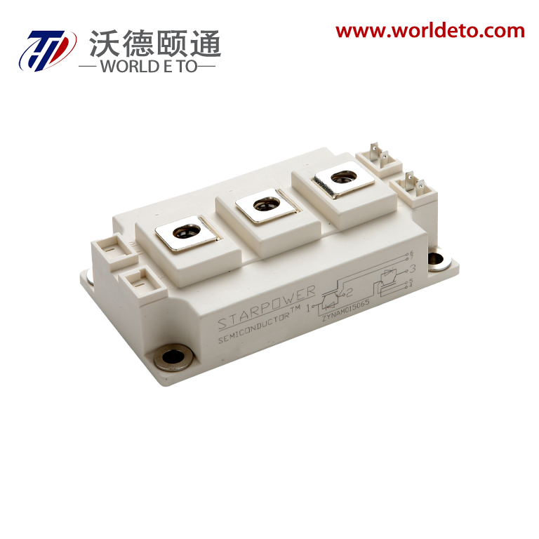
IGBT module, 3-level ,produced by STARPOWER. 1200V 200A.
Features
- Low VCE(sat) Trench IGBT technology
- VCE(sat) with positive temperature coefficient
- Low switching loss
- Maximum junction temperature 175oC
- Low inductance case
- Fast & soft reverse recovery anti-parallel FWD
- Isolated copper baseplate using DBC technology
Typical Applications
- Inverter for motor drive
- Uninterruptible power supply
- Solar power
Absolute Maximum Ratings TC=25oC unless otherwise noted
T1-T4 IGBT
Symbol |
Description |
Value |
Unit |
VCES |
Collector-Emitter Voltage |
1200 |
V |
VGES |
Gate-Emitter Voltage |
±20 |
V |
IC |
Collector Current @ TC=25oC
@ TC= 100oC
|
337
200
|
A |
ICM |
Pulsed Collector Current tp=1ms |
400 |
A |
PD |
Maximum Power Dissipation @ Tj=175oC |
1162 |
W |
D1-D4 Diode
Symbol |
Description |
Value |
Unit |
VRRM |
Repetitive Peak Reverse Voltage |
1200 |
V |
IF |
Diode Continuous Forward Current |
200 |
A |
IFM |
Diode Maximum Forward Current tp=1ms |
400 |
A |
D5,D6 Diode
Symbol |
Description |
Value |
Unit |
VRRM |
Repetitive Peak Reverse Voltage |
1200 |
V |
IF |
Diode Continuous Forward Current |
200 |
A |
IFM |
Diode Maximum Forward Current tp=1ms |
400 |
A |
Module
Symbol |
Description |
Value |
Unit |
Tjmax |
Maximum Junction Temperature |
175 |
oC |
Tjop |
Operating Junction Temperature |
-40 to +150 |
oC |
TSTG |
Storage Temperature Range |
-40 to +125 |
oC |
VISO |
Isolation Voltage RMS,f=50Hz,t=1min |
2500 |
V |
T1-T4 IGBT Characteristics TC=25oC unless otherwise noted
Symbol |
Parameter |
Test Conditions |
Min. |
Typ. |
Max. |
Unit |
|
VCE(sat)
|
Collector to Emitter
Saturation Voltage
|
IC=200A,VGE=15V, Tj=25oC |
|
1.70 |
2.15 |
V
|
IC=200A,VGE=15V, Tj=125oC |
|
1.95 |
|
IC=200A,VGE=15V, Tj=150oC |
|
2.00 |
|
VGE(th) |
Gate-Emitter Threshold Voltage |
IC=5.0mA,VCE=VGE, Tj=25oC |
5.2 |
6.0 |
6.8 |
V |
ICES |
Collector Cut-Off
Current
|
VCE=VCES,VGE=0V,
Tj=25oC
|
|
|
1.0 |
mA |
IGES |
Gate-Emitter Leakage Current |
VGE=VGES,VCE=0V, Tj=25oC |
|
|
400 |
nA |
RGint |
Internal Gate Resistance |
|
|
4.0 |
|
Ω |
Cies |
Input Capacitance |
VCE=25V,f=1MHz,
VGE=0V
|
|
20.7 |
|
nF |
Cres |
Reverse Transfer
Capacitance
|
|
0.58 |
|
nF |
QG |
Gate Charge |
VGE=- 15…+15V |
|
1.55 |
|
μC |
td(on) |
Turn-On Delay Time |
VCC=600V,IC=200A, RG= 1. 1Ω,VGE=±15V, Tj=25oC
|
|
150 |
|
ns |
tr |
Rise Time |
|
32 |
|
ns |
td(off) |
Turn-Off Delay Time |
|
330 |
|
ns |
tf |
Fall Time |
|
93 |
|
ns |
Eon |
Turn-On Switching
Loss
|
|
11.2 |
|
mJ |
Eoff |
Turn-Off Switching
Loss
|
|
11.3 |
|
mJ |
td(on) |
Turn-On Delay Time |
VCC=600V,IC=200A, RG= 1. 1Ω,VGE=±15V, Tj= 125oC
|
|
161 |
|
ns |
tr |
Rise Time |
|
37 |
|
ns |
td(off) |
Turn-Off Delay Time |
|
412 |
|
ns |
tf |
Fall Time |
|
165 |
|
ns |
Eon |
Turn-On Switching
Loss
|
|
19.8 |
|
mJ |
Eoff |
Turn-Off Switching
Loss
|
|
17.0 |
|
mJ |
td(on) |
Turn-On Delay Time |
VCC=600V,IC=200A, RG= 1. 1Ω,VGE=±15V, Tj= 150oC
|
|
161 |
|
ns |
tr |
Rise Time |
|
43 |
|
ns |
td(off) |
Turn-Off Delay Time |
|
433 |
|
ns |
tf |
Fall Time |
|
185 |
|
ns |
Eon |
Turn-On Switching
Loss
|
|
21.9 |
|
mJ |
Eoff |
Turn-Off Switching
Loss
|
|
19.1 |
|
mJ |
|
ISC
|
SC Data
|
tP≤10μs,VGE=15V,
Tj=150oC,VCC=900V, VCEM≤1200V
|
|
800
|
|
A
|
D1-D4 Diode Characteristics TC=25oC unless otherwise noted
Symbol |
Parameter |
Test Conditions |
Min. |
Typ. |
Max. |
Units |
|
VF
|
Diode Forward
Voltage
|
IF=200A,VGE=0V,Tj=25oC |
|
1.65 |
2.10 |
V
|
IF=200A,VGE=0V,Tj= 125oC |
|
1.65 |
|
IF=200A,VGE=0V,Tj= 150oC |
|
1.65 |
|
Qr |
Recovered Charge |
VR=600V,IF=200A,
-di/dt=5400A/μs,VGE=- 15V Tj=25oC
|
|
17.6 |
|
μC |
IRM |
Peak Reverse
Recovery Current
|
|
228 |
|
A |
Erec |
Reverse Recovery Energy |
|
7.7 |
|
mJ |
Qr |
Recovered Charge |
VR=600V,IF=200A,
-di/dt=5400A/μs,VGE=- 15V Tj=125oC
|
|
31.8 |
|
μC |
IRM |
Peak Reverse
Recovery Current
|
|
238 |
|
A |
Erec |
Reverse Recovery Energy |
|
13.8 |
|
mJ |
Qr |
Recovered Charge |
VR=600V,IF=200A,
-di/dt=5400A/μs,VGE=- 15V Tj=150oC
|
|
36.6 |
|
μC |
IRM |
Peak Reverse
Recovery Current
|
|
247 |
|
A |
Erec |
Reverse Recovery Energy |
|
15.2 |
|
mJ |
D5,D6 Diode Characteristics TC=25oC unless otherwise noted
Symbol |
Parameter |
Test Conditions |
Min. |
Typ. |
Max. |
Units |
|
VF
|
Diode Forward
Voltage
|
IF=200A,VGE=0V,Tj=25oC |
|
1.65 |
2.10 |
V
|
IF=200A,VGE=0V,Tj= 125oC |
|
1.65 |
|
IF=200A,VGE=0V,Tj= 150oC |
|
1.65 |
|
Qr |
Recovered Charge |
VR=600V,IF=200A,
-di/dt=5400A/μs,VGE=- 15V Tj=25oC
|
|
17.6 |
|
μC |
IRM |
Peak Reverse
Recovery Current
|
|
228 |
|
A |
Erec |
Reverse Recovery Energy |
|
7.7 |
|
mJ |
Qr |
Recovered Charge |
VR=600V,IF=200A,
-di/dt=5400A/μs,VGE=- 15V Tj=125oC
|
|
31.8 |
|
μC |
IRM |
Peak Reverse
Recovery Current
|
|
238 |
|
A |
Erec |
Reverse Recovery Energy |
|
13.8 |
|
mJ |
Qr |
Recovered Charge |
VR=600V,IF=200A,
-di/dt=5400A/μs,VGE=- 15V Tj=150oC
|
|
36.6 |
|
μC |
IRM |
Peak Reverse
Recovery Current
|
|
247 |
|
A |
Erec |
Reverse Recovery Energy |
|
15.2 |
|
mJ |
NTC Characteristics TC=25oC unless otherwise noted
Symbol |
Parameter |
Test Conditions |
Min. |
Typ. |
Max. |
Unit |
R25 |
Rated Resistance |
|
|
5.0 |
|
kΩ |
ΔR/R |
Deviation of R100 |
TC= 100 oC,R100=493.3Ω |
-5 |
|
5 |
% |
P25 |
Power
Dissipation
|
|
|
|
20.0 |
mW |
B25/50 |
B-value |
R2=R25exp[B25/50(1/T2-
1/(298.15K))]
|
|
3375 |
|
K |
B25/80 |
B-value |
R2=R25exp[B25/80(1/T2-
1/(298.15K))]
|
|
3411 |
|
K |
B25/100 |
B-value |
R2=R25exp[B25/100(1/T2-
1/(298.15K))]
|
|
3433 |
|
K |
Module Characteristics TC=25oC unless otherwise noted
Symbol |
Parameter |
Min. |
Typ. |
Max. |
Unit |
|
RthJC
|
Junction-to-Case (per T1-T4 IGBT)
Junction-to-Case (per D1-D4 Diode)
Junction-to-Case (per D5,D6 Diode)
|
|
|
0.129
0.237
0.232
|
K/W |
|
RthCH
|
Case-to-Heatsink (per T1-T4 IGBT)
Case-to-Heatsink (per D1-D4 Diode)
Case-to-Heatsink (per D5,D6 Diode)
Case-to-Heatsink (per Module)
|
|
0.073
0.134
0.131
0.010
|
|
K/W
|
M |
Terminal Connection Torque, Screw M6 Mounting Torque, Screw M6 |
2.5
3.0
|
|
5.0
5.0
|
|
G |
Weight of Module |
|
340 |
|
g |