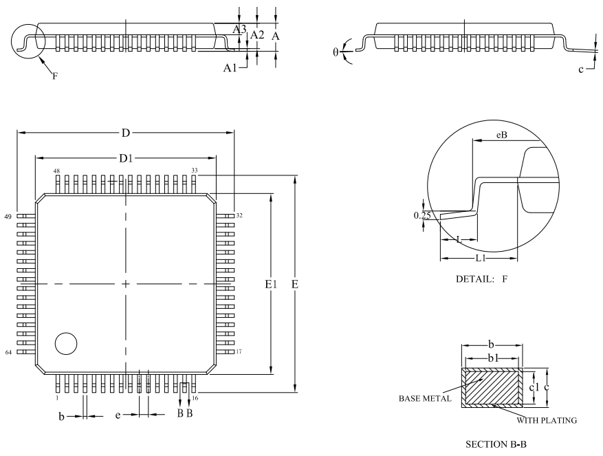
Low Power ADC Solutions: High-Precision Analog-to-Digital Converters for Energy-Efficient Applications

All Categories
Get a Quote

Get a Free Quote

Our representative will contact you soon.
Email
Name
Company Name
Message
0/1000

low power adc

A low power adc represents a critical component in modern electronic systems where energy efficiency meets precision measurement capabilities. This specialized analog-to-digital converter transforms continuous analog signals into discrete digital values while consuming minimal electrical power, making it essential for battery-operated devices and energy-conscious applications. The primary function of a low power adc involves sampling analog voltages at specific intervals and converting these measurements into binary code that microprocessors can interpret and process effectively. These converters typically operate with supply voltages ranging from 1.8V to 5V, consuming microamperes to milliamperes of current depending on sampling rates and resolution requirements. Technological features of modern low power adc units include advanced CMOS fabrication processes that reduce parasitic capacitance and leakage currents significantly. Many designs incorporate delta-sigma modulation techniques that achieve high resolution while maintaining low power consumption through oversampling and noise shaping algorithms. Sleep modes and power-down functionality allow these converters to enter ultra-low power states between measurements, extending battery life in portable applications. Resolution capabilities typically range from 12-bit to 24-bit precision, with sampling rates adjustable from a few samples per second to several kilosamples per second. Applications for low power adc technology span numerous industries and use cases. Medical devices utilize these converters in portable glucose monitors, heart rate sensors, and continuous health monitoring systems where battery longevity is crucial. Industrial automation systems employ low power adc units in wireless sensor networks for environmental monitoring, predictive maintenance applications, and remote data acquisition systems. Consumer electronics integrate these converters in smartwatches, fitness trackers, smartphone sensors, and IoT devices that require extended operational periods without charging or battery replacement.

New Products

The advantages of low power adc technology deliver substantial practical benefits that directly impact product performance and user experience across multiple application domains. Energy efficiency stands as the most significant advantage, enabling devices to operate for months or years on single battery charges. This extended operational life reduces maintenance costs dramatically and improves user satisfaction by eliminating frequent battery replacements or charging cycles. Modern low power adc designs consume as little as 0.5 microamperes in standby mode and under 100 microamperes during active conversion, representing power savings of 90% compared to conventional converters. Cost reduction benefits emerge from decreased battery requirements and simplified power management circuits. Products utilizing low power adc technology can employ smaller batteries or energy harvesting systems, reducing overall bill of materials costs and enabling more compact product designs. The reduced power consumption also minimizes heat generation, eliminating the need for thermal management solutions in many applications and further reducing system complexity and costs. Reliability improvements result from lower operating temperatures and reduced stress on power supply components. Low power adc units experience fewer thermal cycling effects and component degradation over time, leading to longer product lifespans and reduced warranty claims. The stable operation across wide temperature ranges makes these converters suitable for harsh environmental conditions where traditional high-power alternatives might fail. Design flexibility increases significantly with low power adc implementation. Engineers can create wireless sensor networks without complex power distribution infrastructure, enabling deployment in remote or inaccessible locations. The reduced electromagnetic interference from lower power operation simplifies PCB layout requirements and reduces shielding needs. Integration capabilities allow combining multiple sensor inputs with single low power adc units, consolidating measurement functions and reducing overall system complexity. Performance benefits include improved signal integrity through reduced noise coupling and ground bounce effects associated with high current switching. The consistent power draw characteristics of low power adc technology enable more predictable system behavior and simplified power budget calculations during design phases.

Practical Tips

Is Your ADC/DAC Underperforming? The Culprit Could Be Your Voltage Reference

24

Nov

Is Your ADC/DAC Underperforming? The Culprit Could Be Your Voltage Reference

In the realm of precision analog-to-digital and digital-to-analog conversion, engineers often focus on the specifications of the ADC or DAC itself while overlooking a critical component that can make or break system performance. The voltage reference...
View More
High-Accuracy ADC & DAC Chips: The Core of Precision Measurement Systems

07

Jan

High-Accuracy ADC & DAC Chips: The Core of Precision Measurement Systems

In today's advanced measurement and control systems, the bridge between analog real-world signals and digital processing relies heavily on specialized semiconductor components. These critical interface chips, specifically High-Accuracy ADC & DAC Chip...
View More
High-Performance ADC Chips and Precision DACs: Analysis of High-Speed, Low-Power Domestic Alternatives

02

Feb

High-Performance ADC Chips and Precision DACs: Analysis of High-Speed, Low-Power Domestic Alternatives

The semiconductor industry has witnessed unprecedented growth in demand for high-performance analog-to-digital converter chips and precision digital-to-analog converters. As electronic systems become increasingly sophisticated, the need for reliable,...
View More
High-Performance Instrumentation Amplifiers: Minimizing Noise in Low-Level Signal Gain

03

Feb

High-Performance Instrumentation Amplifiers: Minimizing Noise in Low-Level Signal Gain

Modern industrial applications demand exceptional precision when handling low-level signals, making instrumentation amplifiers a cornerstone technology in measurement and control systems. These specialized amplifiers provide high gain while maintaini...
View More

Get a Free Quote

Our representative will contact you soon.
Email
Name
Company Name
Message
0/1000

low power adc

Extended Battery Life Through Ultra-Low Power Consumption

Extended Battery Life Through Ultra-Low Power Consumption

The exceptional energy efficiency of modern low power adc technology fundamentally transforms how electronic devices manage power resources, delivering unprecedented battery life extensions that benefit both manufacturers and end users significantly. Advanced semiconductor fabrication processes enable these converters to achieve standby current consumption as low as 0.5 microamperes while maintaining full operational readiness, representing a dramatic improvement over traditional converter designs that consume hundreds of microamperes continuously. During active conversion periods, optimized low power adc units typically draw between 10 to 100 microamperes depending on sampling rate and resolution settings, allowing precise control over power consumption based on application requirements. This intelligent power management becomes particularly valuable in applications where measurement frequency can be adjusted dynamically based on system conditions or user preferences. The cumulative effect of these power savings translates to battery life extensions ranging from 300% to 1000% compared to conventional analog-to-digital conversion solutions. For example, a wireless sensor node that previously operated for three months on a single battery charge can now function for over two years using the same power source when equipped with appropriate low power adc technology. This dramatic improvement reduces operational costs associated with battery replacement, maintenance visits, and device downtime significantly. Environmental benefits also emerge from reduced battery waste and decreased frequency of service interventions in remote installations. The extended operational periods enable deployment of monitoring systems in previously impractical locations where regular maintenance access is difficult or expensive. Furthermore, the consistent low power draw characteristics allow for integration with energy harvesting systems such as solar panels, thermal generators, or vibration harvesters, potentially enabling completely self-sustaining operation in appropriate environments. System designers appreciate the predictable power consumption profiles that facilitate accurate power budget calculations and enable optimization of overall energy management strategies throughout product development cycles.
Precision Measurement Capabilities with Minimal System Impact

Precision Measurement Capabilities with Minimal System Impact

The remarkable precision measurement capabilities of low power adc technology deliver exceptional accuracy and resolution while maintaining minimal impact on overall system performance and resources, establishing these converters as ideal solutions for demanding measurement applications where both precision and efficiency are critical requirements. Modern low power adc designs achieve resolution levels ranging from 16-bit to 24-bit precision, providing measurement granularity sufficient for the most demanding sensor applications including medical diagnostics, environmental monitoring, and scientific instrumentation. The high resolution capabilities enable detection of minute signal variations that might indicate critical system conditions or early warning signs of equipment degradation, supporting predictive maintenance strategies and improving overall system reliability. Advanced oversampling techniques employed in delta-sigma low power adc architectures effectively increase the signal-to-noise ratio without proportionally increasing power consumption, delivering measurement quality comparable to much higher power converter designs. The integration of programmable gain amplifiers and flexible input multiplexing allows single low power adc units to handle multiple sensor inputs with varying signal levels and characteristics, reducing component count and simplifying system design complexity significantly. Calibration capabilities built into many low power adc designs enable compensation for temperature drift, reference voltage variations, and aging effects, maintaining measurement accuracy over extended operational periods without external intervention. The stable performance characteristics across wide temperature ranges ensure consistent measurement quality in harsh environmental conditions where traditional converters might experience degraded accuracy or complete failure. Digital filtering and signal processing capabilities integrated within advanced low power adc designs provide additional noise reduction and signal conditioning without requiring external processing resources, further minimizing system impact while maximizing measurement quality. The combination of high precision, low power consumption, and integrated signal processing creates compelling value propositions for applications where measurement quality cannot be compromised despite strict energy budget constraints.
Flexible Integration and Scalable Design Architecture

Flexible Integration and Scalable Design Architecture

The inherent flexibility and scalable design architecture of modern low power adc technology provides unprecedented opportunities for system integration and customization, enabling engineers to create tailored solutions that precisely match application requirements while minimizing development time and complexity throughout the design process. Advanced communication interfaces including SPI, I2C, and UART protocols facilitate seamless integration with virtually any microcontroller or digital signal processor, eliminating compatibility concerns and reducing interface circuit requirements significantly. The standardized command structures and register maps common across low power adc product families enable rapid prototyping and simplified software development, allowing engineers to leverage existing code libraries and development tools effectively. Programmable operating parameters including sampling rate, resolution, input range, and power management modes provide extensive customization capabilities without requiring hardware modifications, enabling single converter designs to serve multiple application requirements efficiently. This configurability reduces inventory complexity for manufacturers and provides valuable design margin for accommodating evolving specifications or performance requirements during product development cycles. Multi-channel input capabilities with programmable gain settings allow individual optimization of each measurement channel, supporting diverse sensor types and signal levels within unified system architectures. The ability to dynamically reconfigure operating parameters through software control enables adaptive measurement strategies that can optimize performance based on real-time conditions or user preferences, maximizing both measurement quality and energy efficiency simultaneously. Reference voltage options including internal precision references and external reference inputs provide flexibility for achieving specific accuracy requirements or matching existing system voltage standards without additional circuitry. Clock generation and timing control features enable synchronization with external events or coordination among multiple converter units in distributed measurement systems. The robust design architecture of low power adc technology includes comprehensive protection features such as overvoltage detection, thermal shutdown, and electrostatic discharge protection, ensuring reliable operation in challenging environments while minimizing the need for external protection components and reducing overall system vulnerability to environmental stresses.

Get a Free Quote

Our representative will contact you soon.
Email
Name
Company Name
Message
0/1000