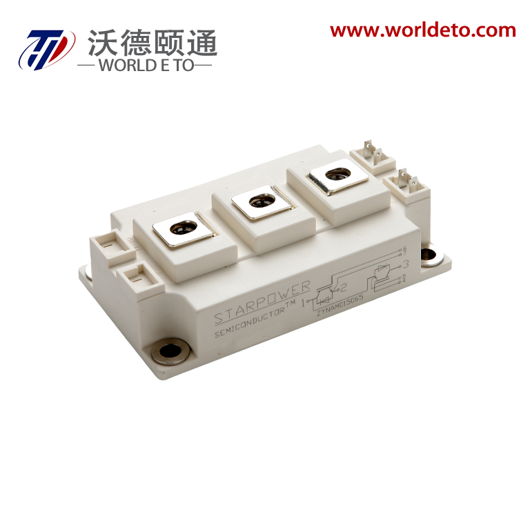
Brief introduction
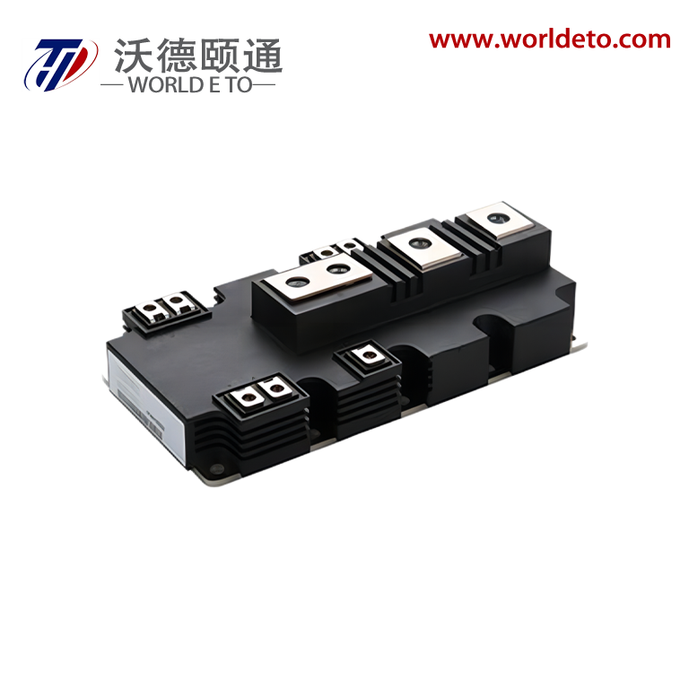
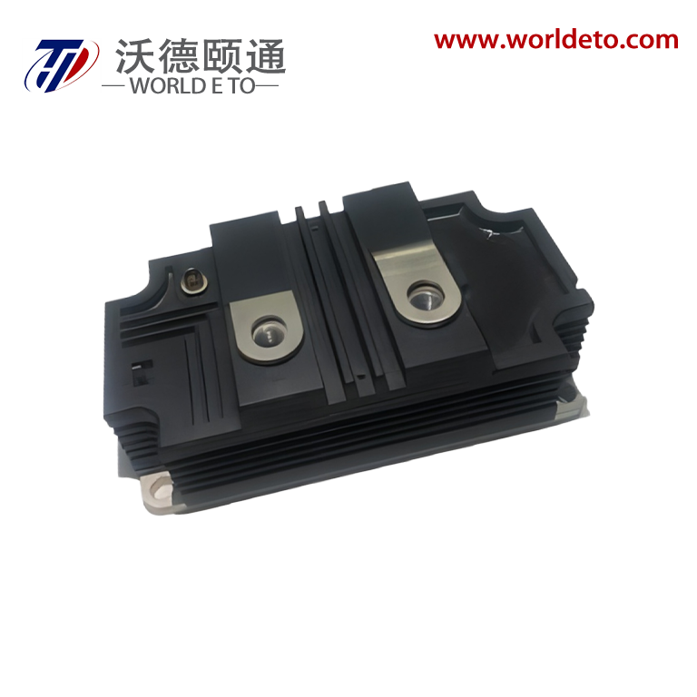
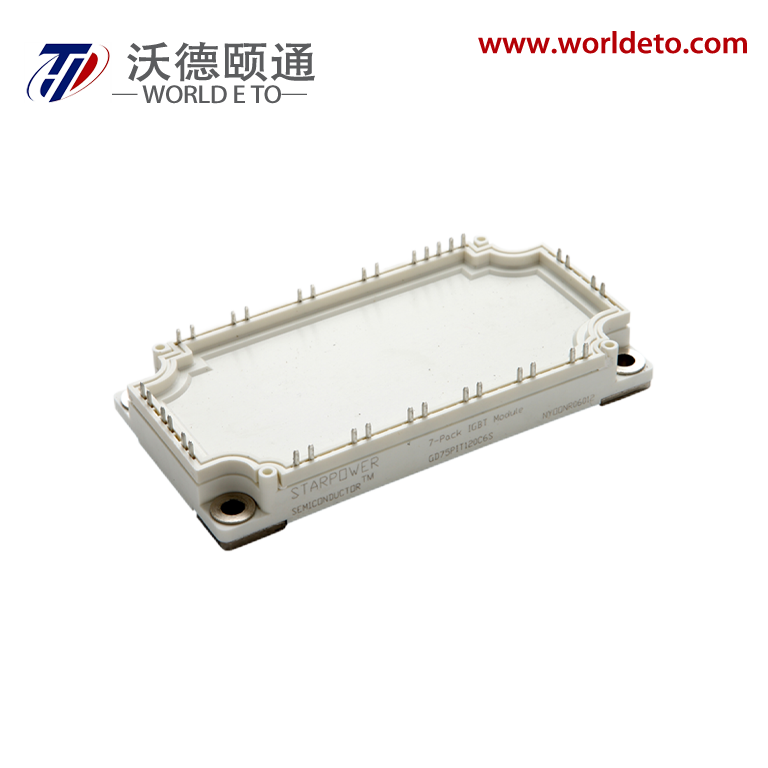
IGBT module, produced by STARPOWER. 1700V 650A
Features
-
Low VCE(sat) Trench IGBT technology
-
10μs short circuit capability
-
VCE(sat) with positive temperature coefficient
-
Maximum junction temperature 175oC
-
Enlarged Diode for regenerative operation
- Isolated copper baseplate using DBC technology
-
High power and thermal cycling capability
Typical Applications
- High Power Converter
- Wind and Solar Power
- Traction Drive
Absolute Maximum Ratings TC=25oC unless otherwise note
IGBT
Symbol |
Description |
Value |
Unit |
VCES |
Collector-Emitter Voltage |
1700 |
V |
VGES |
Gate-Emitter Voltage |
±20 |
V |
IC |
Collector Current @ TC=25oC
@ TC= 100oC
|
1073
650
|
A |
ICM |
Pulsed Collector Current tp=1ms |
1300 |
A |
PD |
Maximum Power Dissipation @ Tj=175oC |
4.2 |
kW |
Diode
Symbol |
Description |
Value |
Unit |
VRRM |
Repetitive Peak Reverse Voltage |
1700 |
V |
IF |
Diode Continuous Forward Current |
650 |
A |
IFM |
Diode Maximum Forward Current tp=1ms |
1300 |
A |
Module
Symbol |
Description |
Value |
Unit |
Tjmax |
Maximum Junction Temperature |
175 |
oC |
Tjop |
Operating Junction Temperature |
-40 to +150 |
oC |
TSTG |
Storage Temperature Range |
-40 to +150 |
oC |
VISO |
Isolation Voltage RMS,f=50Hz,t=1min |
4000 |
V |
IGBT Characteristics TC=25oC unless otherwise noted
Symbol |
Parameter |
Test Conditions |
Min. |
Typ. |
Max. |
Unit |
|
VCE(sat)
|
Collector to Emitter
Saturation Voltage
|
IC=650A,VGE=15V, Tj=25oC |
|
1.90 |
2.35 |
V
|
IC=650A,VGE=15V, Tj=125oC |
|
2.35 |
|
IC=650A,VGE=15V, Tj=150oC |
|
2.45 |
|
VGE(th) |
Gate-Emitter Threshold Voltage |
IC=24.0mA,VCE=VGE, Tj=25oC |
5.6 |
6.2 |
6.8 |
V |
ICES |
Collector Cut-Off
Current
|
VCE=VCES,VGE=0V,
Tj=25oC
|
|
|
5.0 |
mA |
IGES |
Gate-Emitter Leakage Current |
VGE=VGES,VCE=0V, Tj=25oC |
|
|
400 |
nA |
RGint |
Internal Gate Resistance |
|
|
2.3 |
|
Ω |
Cies |
Input Capacitance |
VCE=25V,f=1MHz,
VGE=0V
|
|
72.3 |
|
nF |
Cres |
Reverse Transfer
Capacitance
|
|
1.75 |
|
nF |
QG |
Gate Charge |
VGE=- 15…+15V |
|
5.66 |
|
μC |
td(on) |
Turn-On Delay Time |
VCC=900V,IC=650A, RGon= 1.8Ω,RGoff=2.7Ω, VGE=±15V,Tj=25oC
|
|
468 |
|
ns |
tr |
Rise Time |
|
86 |
|
ns |
td(off) |
Turn-Off Delay Time |
|
850 |
|
ns |
tf |
Fall Time |
|
363 |
|
ns |
Eon |
Turn-On Switching
Loss
|
|
226 |
|
mJ |
Eoff |
Turn-Off Switching
Loss
|
|
161 |
|
mJ |
td(on) |
Turn-On Delay Time |
VCC=900V,IC=650A, RGon= 1.8Ω,RGoff=2.7Ω, VGE=±15V,Tj= 125oC
|
|
480 |
|
ns |
tr |
Rise Time |
|
110 |
|
ns |
td(off) |
Turn-Off Delay Time |
|
1031 |
|
ns |
tf |
Fall Time |
|
600 |
|
ns |
Eon |
Turn-On Switching
Loss
|
|
338 |
|
mJ |
Eoff |
Turn-Off Switching
Loss
|
|
226 |
|
mJ |
td(on) |
Turn-On Delay Time |
VCC=900V,IC=650A, RGon= 1.8Ω,RGoff=2.7Ω, VGE=±15V,Tj= 150oC
|
|
480 |
|
ns |
tr |
Rise Time |
|
120 |
|
ns |
td(off) |
Turn-Off Delay Time |
|
1040 |
|
ns |
tf |
Fall Time |
|
684 |
|
ns |
Eon |
Turn-On Switching
Loss
|
|
368 |
|
mJ |
Eoff |
Turn-Off Switching
Loss
|
|
242 |
|
mJ |
|
ISC
|
SC Data
|
tP≤10μs,VGE=15V,
Tj=150oC,VCC= 1000V, VCEM≤1700V
|
|
2600
|
|
A
|
Diode Characteristics TC=25oC unless otherwise noted
Symbol |
Parameter |
Test Conditions |
Min. |
Typ. |
Max. |
Unit |
|
VF
|
Diode Forward
Voltage
|
IF=650A,VGE=0V,Tj=25oC |
|
1.85 |
2.30 |
V
|
IF=650A,VGE=0V,Tj= 125oC |
|
1.98 |
|
IF=650A,VGE=0V,Tj= 150oC |
|
2.02 |
|
Qr |
Recovered Charge |
VR=900V,IF=650A,
-di/dt=5980A/μs,VGE=- 15V Tj=25oC
|
|
176 |
|
μC |
IRM |
Peak Reverse
Recovery Current
|
|
765 |
|
A |
Erec |
Reverse Recovery Energy |
|
87.4 |
|
mJ |
Qr |
Recovered Charge |
VR=900V,IF=650A,
-di/dt=5980A/μs,VGE=- 15V Tj= 125oC
|
|
292 |
|
μC |
IRM |
Peak Reverse
Recovery Current
|
|
798 |
|
A |
Erec |
Reverse Recovery Energy |
|
159 |
|
mJ |
Qr |
Recovered Charge |
VR=900V,IF=650A,
-di/dt=5980A/μs,VGE=- 15V Tj= 150oC
|
|
341 |
|
μC |
IRM |
Peak Reverse
Recovery Current
|
|
805 |
|
A |
Erec |
Reverse Recovery Energy |
|
192 |
|
mJ |
NTC Characteristics TC=25oC unless otherwise noted
Symbol |
Parameter |
Test Conditions |
Min. |
Typ. |
Max. |
Unit |
R25 |
Rated Resistance |
|
|
5.0 |
|
kΩ |
ΔR/R |
Deviation of R100 |
TC= 100 oC,R100=493.3Ω |
-5 |
|
5 |
% |
P25 |
Power
Dissipation
|
|
|
|
20.0 |
mW |
B25/50 |
B-value |
R2=R25exp[B25/50(1/T2-
1/(298.15K))]
|
|
3375 |
|
K |
B25/80 |
B-value |
R2=R25exp[B25/80(1/T2-
1/(298.15K))]
|
|
3411 |
|
K |
B25/100 |
B-value |
R2=R25exp[B25/100(1/T2-
1/(298.15K))]
|
|
3433 |
|
K |
Module Characteristics TC=25oC unless otherwise noted
Symbol |
Parameter |
Min. |
Typ. |
Max. |
Unit |
LCE |
Stray Inductance |
|
18 |
|
nH |
RCC’+EE’ |
Module Lead Resistance, Terminal to Chip |
|
0.30 |
|
mΩ |
RthJC |
Junction-to-Case (per IGBT)
Junction-to-Case (per Diode)
|
|
|
35.8
71.3
|
K/kW |
|
RthCH
|
Case-to-Heatsink (per IGBT)
Case-to-Heatsink (per Diode)
Case-to-Heatsink (per Module)
|
|
13.5
26.9
4.5
|
|
K/kW |
|
M
|
Terminal Connection Torque, Screw M4 Terminal Connection Torque, Screw M8 Mounting Torque, Screw M5 |
1.8
8.0
3.0
|
|
2.1
10.0
6.0
|
N.m
|
G |
Weight of Module |
|
810 |
|
g |