MOSFET Low Voltage: High-Performance Power Switching Solutions for Efficient Electronic Systems

All Categories
Get a Quote

Get a Free Quote

Our representative will contact you soon.
Email
Name
Company Name
Message
0/1000

mosfet low voltage

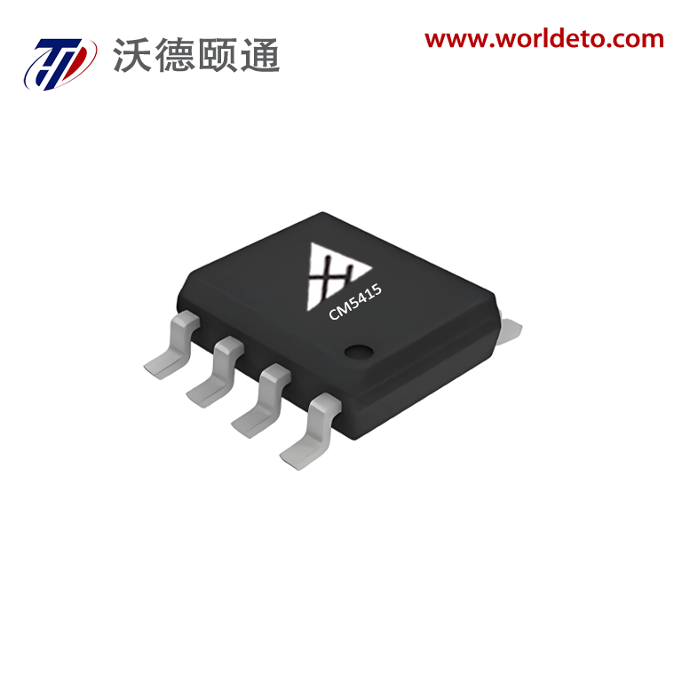
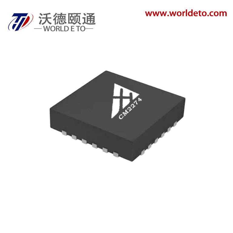
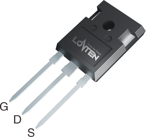
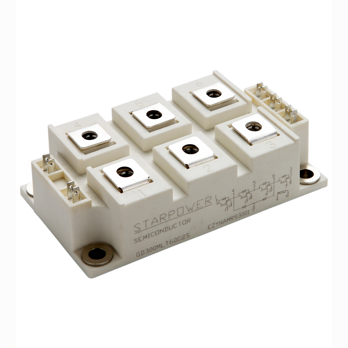
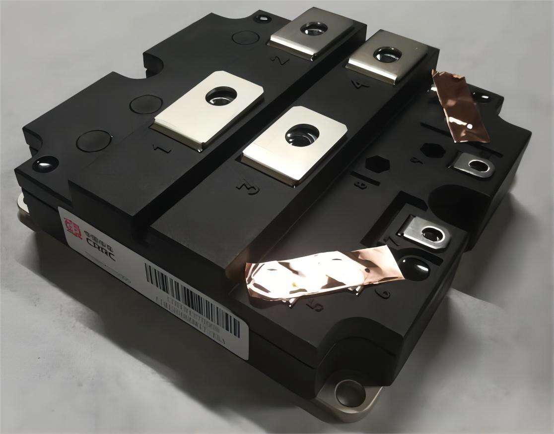
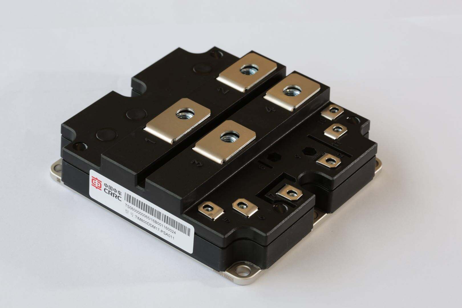
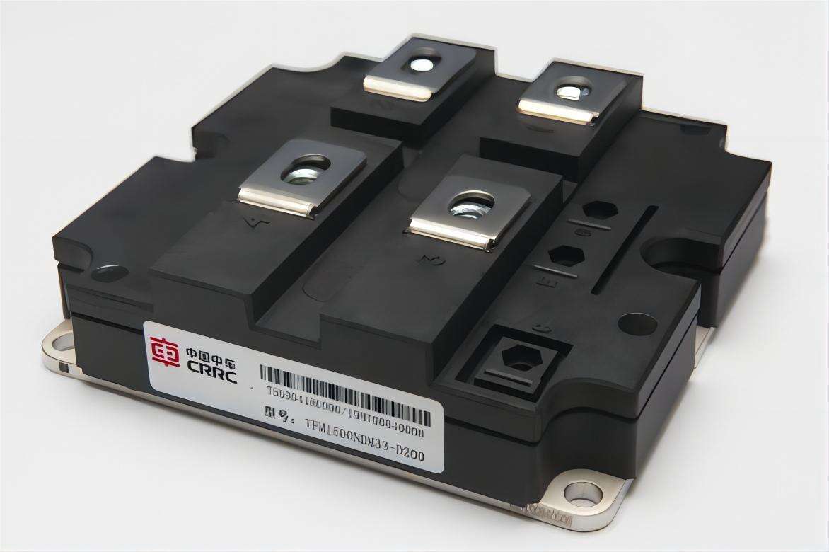
The mosfet low voltage represents a revolutionary advancement in power semiconductor technology, specifically designed to operate efficiently in applications requiring reduced voltage levels. This specialized metal-oxide-semiconductor field-effect transistor delivers exceptional performance while maintaining energy efficiency across diverse electronic systems. The mosfet low voltage incorporates advanced silicon technology that enables superior switching characteristics at voltages typically ranging from 12V to 60V, making it ideal for modern electronic designs where power conservation and reliability are paramount. Its sophisticated gate structure allows for precise control over current flow, ensuring optimal power management in sensitive applications. The technological features of the mosfet low voltage include ultra-low on-resistance characteristics that minimize power losses during operation. This component utilizes innovative manufacturing processes that create exceptionally clean silicon interfaces, resulting in reduced leakage currents and enhanced thermal stability. The device features optimized threshold voltages that enable reliable switching at lower gate drive voltages, significantly reducing the complexity of drive circuitry requirements. Advanced packaging technologies ensure excellent thermal dissipation while maintaining compact form factors suitable for space-constrained applications. The mosfet low voltage finds extensive applications across automotive electronics, portable devices, battery management systems, and renewable energy installations. In automotive applications, these components power LED lighting systems, motor control units, and advanced driver assistance systems where efficiency and reliability are critical. Consumer electronics benefit from the mosfet low voltage in laptop power supplies, smartphone charging circuits, and gaming console power management systems. Industrial automation systems leverage these components for servo motor drives, robotics control systems, and precision instrumentation. Solar inverters and battery charging systems utilize the mosfet low voltage to maximize energy conversion efficiency while minimizing heat generation, contributing to sustainable energy solutions and extended operational lifespans.

New Product Recommendations

The mosfet low voltage delivers substantial benefits that make it the preferred choice for engineers and system designers seeking optimal performance in power management applications. Energy efficiency stands as the primary advantage, with these components achieving conversion efficiencies exceeding 95 percent in many applications. This exceptional efficiency translates directly into reduced operating costs, lower heat generation, and extended battery life in portable devices. The superior thermal characteristics of the mosfet low voltage eliminate the need for complex cooling systems in many applications, reducing both component costs and system complexity. Reliability represents another significant advantage of the mosfet low voltage technology. These components demonstrate exceptional durability under demanding operating conditions, with mean time between failures often exceeding 100,000 hours in typical applications. The robust construction and advanced materials used in manufacturing ensure consistent performance across wide temperature ranges, from -55°C to +175°C, making them suitable for harsh environmental conditions. The fast switching capabilities of the mosfet low voltage enable precise control in dynamic applications while minimizing switching losses that typically plague conventional power devices. Design flexibility emerges as a crucial advantage when implementing mosfet low voltage solutions. These components offer engineers greater freedom in circuit design due to their low gate drive requirements and compatibility with standard logic voltage levels. The reduced electromagnetic interference generated by mosfet low voltage devices simplifies compliance with regulatory standards while improving overall system performance. Their compact package options enable miniaturization of power supplies and control systems without sacrificing performance or reliability. Cost-effectiveness becomes apparent when considering the total system benefits of mosfet low voltage implementation. While initial component costs may be comparable to alternatives, the reduced need for heat sinks, simplified drive circuits, and improved reliability result in lower total cost of ownership. Manufacturing benefits include simplified assembly processes, reduced testing requirements, and improved yield rates due to the inherent robustness of mosfet low voltage technology. The widespread availability and standardization of these components ensure supply chain stability and competitive pricing across various market segments.

Tips And Tricks

Accuracy, Drift, and Noise: The Key Specifications of Precision Voltage References

24

Nov

Accuracy, Drift, and Noise: The Key Specifications of Precision Voltage References

In the world of electronic circuit design and measurement systems, precision voltage references serve as the cornerstone for achieving accurate and reliable performance. These critical components provide stable reference voltages that enable precise ...
View More
From ADC to LDO: Complete High-Precision, Low-Power Domestic Chip Replacement Solutions

02

Feb

From ADC to LDO: Complete High-Precision, Low-Power Domestic Chip Replacement Solutions

The semiconductor industry faces unprecedented challenges as global supply chain disruptions and geopolitical tensions drive demand for reliable domestic chip replacement solutions. Companies across industries are increasingly seeking alternatives to...
View More
Super-junction MOSFET

25

Jan

Super-junction MOSFET

The super-junction MOSFET (Meta Oxide Semiconductor Field Effect Transistor) introduces a lateral electric field control on the basis of the traditional VDMOS, thereby making the vertical electric field distribution approach an ideal rectangle. This ...
View More
The Best Domestic Alternatives for High-Performance ADC and DAC Chips in 2026

03

Feb

The Best Domestic Alternatives for High-Performance ADC and DAC Chips in 2026

The semiconductor industry is experiencing unprecedented demand for high-performance analog-to-digital converter and digital-to-analog converter solutions, driving engineers and procurement teams to seek reliable domestic alternatives for ADC and DAC...
View More

Get a Free Quote

Our representative will contact you soon.
Email
Name
Company Name
Message
0/1000

mosfet low voltage

Superior Energy Efficiency and Thermal Management

Superior Energy Efficiency and Thermal Management

The mosfet low voltage excels in energy efficiency through its revolutionary low on-resistance design, which dramatically reduces conduction losses during operation. This advanced characteristic enables the device to convert electrical energy with minimal waste heat generation, achieving efficiency levels that often exceed 98 percent in optimized circuit configurations. The superior thermal management capabilities stem from the innovative silicon crystal structure and advanced manufacturing processes that create exceptionally clean semiconductor interfaces. These clean interfaces significantly reduce parasitic resistances and minimize energy losses that would otherwise manifest as unwanted heat generation. The mosfet low voltage incorporates specialized thermal design features, including optimized die attachment methods and enhanced package thermal interfaces that facilitate rapid heat dissipation to the surrounding environment. This exceptional thermal performance eliminates the need for elaborate cooling systems in many applications, reducing both system complexity and overall costs. The device maintains consistent performance characteristics across wide temperature ranges, ensuring reliable operation even in demanding thermal environments. Engineers benefit from simplified thermal design requirements, as the mosfet low voltage naturally operates at lower junction temperatures compared to conventional alternatives. This thermal advantage extends component lifespan significantly, often doubling operational lifetime compared to traditional power switching devices. The reduced thermal stress also improves long-term reliability and reduces maintenance requirements in critical applications. Manufacturing processes incorporate advanced techniques that optimize the crystal lattice structure, resulting in uniform current distribution and minimized hot spots that could compromise device reliability. The combination of low thermal generation and excellent heat dissipation capabilities makes the mosfet low voltage ideal for high-density power conversion systems where thermal management presents significant challenges.
Fast Switching Performance and Electromagnetic Compatibility

Fast Switching Performance and Electromagnetic Compatibility

The mosfet low voltage demonstrates exceptional switching performance through its optimized gate structure and reduced parasitic capacitances, enabling switching frequencies well above conventional power devices while maintaining efficiency and reliability. This fast switching capability results from innovative manufacturing techniques that minimize gate charge requirements and reduce switching transition times. The device achieves rise and fall times measured in nanoseconds, enabling precise control in high-frequency applications such as resonant converters and advanced motor control systems. The reduced switching losses associated with fast transitions contribute significantly to overall system efficiency while enabling compact power supply designs. The electromagnetic compatibility advantages of the mosfet low voltage stem from its controlled switching characteristics and reduced dv/dt rates during transitions. These controlled switching properties minimize electromagnetic interference generation, simplifying compliance with stringent regulatory standards across various industries. The device incorporates design features that reduce parasitic inductances and optimize current commutation paths, resulting in cleaner switching waveforms with minimal ringing and overshoot. Engineers benefit from simplified EMI filtering requirements, often reducing the size and cost of input and output filter components. The improved electromagnetic performance enables higher switching frequencies without compromising system reliability or increasing electromagnetic emissions. Advanced packaging technologies incorporate integrated gate resistors and optimized lead frame designs that further enhance switching performance while maintaining electromagnetic compatibility. The mosfet low voltage enables designers to implement more aggressive switching strategies, resulting in smaller magnetic components and improved power density. This switching performance advantage becomes particularly valuable in space-constrained applications where size and weight considerations are critical. The controlled switching characteristics also reduce stress on associated components, extending overall system reliability and reducing maintenance requirements in mission-critical applications.
Versatile Design Integration and Cost-Effective Implementation

Versatile Design Integration and Cost-Effective Implementation

The mosfet low voltage offers exceptional design integration flexibility through its compatibility with standard control circuits and logic voltage levels, eliminating the need for specialized driver circuits in many applications. This compatibility advantage stems from the optimized threshold voltage characteristics that enable reliable switching with gate drive voltages as low as 5V, making direct interface with microcontrollers and digital signal processors straightforward and cost-effective. The device supports various package configurations, from surface-mount options suitable for automated assembly to through-hole variants for prototype development and specialized applications. This packaging diversity enables engineers to select optimal configurations based on thermal requirements, assembly constraints, and cost considerations. The standardized pinout configurations ensure drop-in compatibility with existing designs while providing pathways for performance upgrades without extensive circuit modifications. Manufacturing advantages include simplified assembly processes due to the robust nature of the mosfet low voltage and its tolerance to handling variations during production. The device demonstrates excellent process compatibility with standard semiconductor manufacturing equipment, ensuring high yield rates and consistent quality across production volumes. Cost-effectiveness emerges through multiple factors including reduced component count due to simplified drive requirements, elimination of complex cooling systems, and improved overall system reliability that reduces warranty and maintenance costs. The mosfet low voltage enables system designers to achieve higher integration levels while maintaining design flexibility for future enhancements and modifications. Supply chain benefits include widespread availability from multiple qualified manufacturers, ensuring competitive pricing and reliable sourcing across various market conditions. The standardization of electrical characteristics and performance parameters simplifies qualification processes and reduces development time for new products. Long-term cost advantages include extended operational lifespans, reduced maintenance requirements, and improved energy efficiency that translates to lower operating costs throughout the product lifecycle. These comprehensive advantages make the mosfet low voltage an attractive solution for both cost-sensitive consumer applications and high-reliability industrial systems.

Get a Free Quote

Our representative will contact you soon.
Email
Name
Company Name
Message
0/1000