High-Performance DAC Wafer Die Solutions - Advanced Digital-to-Analog Conversion Technology

All Categories
Get a Quote

Get a Free Quote

Our representative will contact you soon.
Email
Name
Company Name
Message
0/1000

dac wafer die

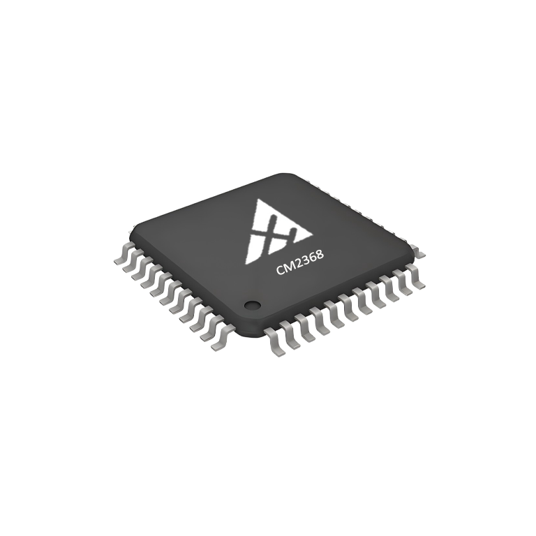
A DAC wafer die represents a fundamental component in modern electronics, serving as the core element that converts digital signals into analog outputs. This semiconductor device operates at the wafer level, providing manufacturers with exceptional flexibility in system integration and design optimization. The DAC wafer die functions by receiving digital input data and transforming it into corresponding analog voltage or current signals through precise electronic circuitry. The conversion process relies on sophisticated algorithms and high-precision resistor networks that ensure accurate signal reproduction across various frequency ranges. Modern DAC wafer die technology incorporates advanced fabrication techniques, utilizing cutting-edge lithography processes to achieve remarkable precision in component placement and electrical characteristics. These devices typically feature multiple resolution options, ranging from 8-bit to 32-bit conversion capabilities, allowing engineers to select the appropriate specification for their specific application requirements. The technological architecture of a DAC wafer die includes multiple critical components: reference voltage circuits, digital input interfaces, conversion logic, and analog output stages. Each element works harmoniously to deliver consistent performance across varying operating conditions. The reference voltage system provides stable baseline measurements, while the digital interface ensures reliable communication with controlling microprocessors or digital signal processors. Temperature compensation circuits maintain accuracy across industrial temperature ranges, making the DAC wafer die suitable for demanding environmental conditions. Manufacturing processes for DAC wafer die production involve sophisticated clean room facilities and precision equipment to maintain tight tolerance specifications. Quality control measures include extensive testing protocols that verify conversion accuracy, linearity, and thermal stability. Applications for DAC wafer die technology span numerous industries, including telecommunications infrastructure, automotive systems, medical devices, industrial automation equipment, and consumer electronics. In telecommunications, these components enable precise signal conditioning for high-speed data transmission. Automotive applications utilize DAC wafer die technology for engine management systems, audio processing, and sensor interface circuits.

New Product Recommendations

The DAC wafer die offers significant advantages that make it an essential component for modern electronic system design. First, the compact form factor provides exceptional space efficiency, allowing engineers to integrate multiple functions within limited board real estate. This miniaturization benefit becomes particularly valuable in portable devices and densely packed electronic assemblies where every millimeter matters. The reduced size also contributes to lower overall system weight, which proves crucial for aerospace, automotive, and mobile applications. Cost effectiveness represents another major advantage, as the DAC wafer die eliminates the need for external packaging traditionally required with discrete components. This packaging reduction translates directly into material cost savings and simplified supply chain management. Manufacturing volumes benefit from economies of scale, making the DAC wafer die an attractive option for high-volume production scenarios. The streamlined production process reduces assembly time and minimizes potential failure points associated with multiple component interconnections. Performance characteristics of the DAC wafer die exceed traditional alternatives through improved signal integrity and reduced parasitic effects. The shorter signal paths inherent in wafer-level integration minimize electromagnetic interference and crosstalk, resulting in cleaner analog outputs and better overall system performance. Power consumption advantages emerge from optimized circuit designs that eliminate unnecessary buffering stages and reduce switching losses. Lower power requirements extend battery life in portable applications and reduce thermal management challenges in high-density systems. The DAC wafer die also provides enhanced reliability through reduced interconnection complexity and improved thermal characteristics. Fewer solder joints and wire bonds decrease the probability of mechanical failure, while the monolithic construction offers superior resistance to vibration and shock. Temperature cycling performance improves due to matched thermal expansion coefficients within the integrated structure. Flexibility in system design increases substantially with DAC wafer die implementation, as engineers can customize interface circuits and optimize performance parameters for specific applications. The ability to integrate multiple DAC channels on a single die enables complex multi-channel systems while maintaining synchronization and reducing component count. Quality control benefits from wafer-level testing capabilities that allow comprehensive characterization before final assembly, ensuring higher yields and more consistent performance across production lots.

Latest News

Low-Power Design Secrets: Utilizing Precision LDOs and Voltage References for Extended Battery Life

07

Jan

Low-Power Design Secrets: Utilizing Precision LDOs and Voltage References for Extended Battery Life

Modern electronic systems demand increasingly sophisticated power management strategies to achieve extended battery life while maintaining optimal performance. The integration of precision LDOs and voltage references has become a cornerstone of effic...
View More
Speed Meets Accuracy: Selecting High-Speed Data Converters for Demanding Applications

07

Jan

Speed Meets Accuracy: Selecting High-Speed Data Converters for Demanding Applications

In today's rapidly evolving industrial landscape, the demand for high-speed data converters has reached unprecedented levels. These critical components serve as the bridge between analog and digital domains, enabling sophisticated control systems to ...
View More
Precision DAC Chips: Achieving Sub-Millivolt Accuracy in Complex Control Systems

03

Feb

Precision DAC Chips: Achieving Sub-Millivolt Accuracy in Complex Control Systems

Modern industrial control systems demand unprecedented accuracy and reliability, with precision DAC chips serving as critical components that bridge the digital-analog divide. These sophisticated semiconductor devices enable engineers to achieve sub-...
View More
Breaking Speed Barriers: The Future of High-Speed ADCs in Modern Communication

03

Feb

Breaking Speed Barriers: The Future of High-Speed ADCs in Modern Communication

The telecommunications industry continues to push the boundaries of data transmission speeds, driving unprecedented demand for advanced analog-to-digital conversion technologies. High-speed ADCs have emerged as the cornerstone of modern communication...
View More

Get a Free Quote

Our representative will contact you soon.
Email
Name
Company Name
Message
0/1000

dac wafer die

Superior Integration Density and Miniaturization

Superior Integration Density and Miniaturization

The DAC wafer die delivers unmatched integration density that revolutionizes electronic system design by combining multiple conversion channels and supporting circuitry onto a single semiconductor substrate. This advanced integration approach eliminates the traditional constraints associated with discrete component layouts, enabling engineers to achieve unprecedented functionality within extremely compact footprints. The miniaturization benefits extend far beyond simple space savings, as the reduced interconnection lengths significantly improve electrical performance by minimizing parasitic capacitance and inductance effects that typically degrade signal quality in conventional designs. Modern DAC wafer die technology achieves remarkable channel density, with some implementations supporting 16 or more independent conversion channels on dies measuring less than 5mm square. This exceptional density becomes particularly valuable in applications such as multi-channel data acquisition systems, advanced audio processing equipment, and sophisticated control systems where space constraints demand maximum functionality per unit area. The integration approach also enables precise matching between channels, as all conversion elements undergo identical fabrication processes and operate under matching thermal conditions. This inherent matching characteristic proves essential for applications requiring high channel-to-channel accuracy, such as precision instrumentation and high-fidelity audio systems. Furthermore, the monolithic construction eliminates variations typically introduced by component tolerances and assembly processes, resulting in superior overall system performance. The manufacturing advantages of wafer-level integration include simplified assembly processes, reduced material costs, and improved yield rates compared to multi-component alternatives. Testing and calibration procedures benefit from the ability to characterize all channels simultaneously, ensuring consistent performance across the entire device. The thermal advantages of integration density include improved heat dissipation through the shared substrate and reduced hot spots that occur with discrete component clustering. This thermal efficiency enables higher performance operation while maintaining reliability standards essential for demanding applications.
Enhanced Signal Integrity and Performance Optimization

Enhanced Signal Integrity and Performance Optimization

The DAC wafer die architecture delivers exceptional signal integrity through carefully optimized circuit layouts and advanced noise reduction techniques that surpass the capabilities of traditional discrete component implementations. The monolithic design approach enables precise control over signal routing, ground plane distribution, and power supply isolation, resulting in significantly reduced noise levels and improved dynamic range performance. Internal signal paths benefit from minimal parasitic effects, as the short interconnection distances and controlled impedance characteristics eliminate many sources of signal degradation commonly encountered in multi-component systems. Advanced design techniques incorporate dedicated analog and digital supply domains with sophisticated isolation barriers that prevent digital switching noise from contaminating sensitive analog conversion circuits. The result is measurably improved signal-to-noise ratios, reduced total harmonic distortion, and enhanced spurious-free dynamic range compared to equivalent discrete solutions. Precision matching of critical components becomes achievable through the controlled fabrication environment, ensuring that resistor networks, current sources, and reference circuits maintain tight tolerances that would be impossible to achieve with discrete components. This precision matching directly translates into improved conversion accuracy, better linearity performance, and enhanced temperature stability across the entire operating range. The DAC wafer die also incorporates advanced compensation circuits that automatically adjust for process variations and environmental changes, maintaining consistent performance without requiring external calibration procedures. Clock distribution networks within the die utilize sophisticated phase-locked loop circuits and low-jitter distribution techniques that ensure precise timing relationships between conversion channels. This timing precision becomes critical for applications requiring synchronized multi-channel operation or high-speed conversion rates where timing uncertainties would degrade system performance. The optimized power management systems within the DAC wafer die include intelligent power sequencing, voltage regulation, and current limiting functions that protect the device while maximizing performance efficiency. These integrated protection mechanisms eliminate the need for external protection circuits while ensuring reliable operation under varying load conditions.
Versatile Application Compatibility and System Integration

Versatile Application Compatibility and System Integration

The DAC wafer die demonstrates exceptional versatility through its comprehensive interface options and configurable operating modes that accommodate diverse application requirements across multiple industries and system architectures. This adaptability stems from sophisticated digital interface protocols that support popular communication standards including SPI, I2C, and parallel interfaces, enabling seamless integration with virtually any microcontroller or digital signal processor platform. The flexible configuration options allow engineers to optimize conversion parameters such as update rates, output ranges, and power consumption levels to match specific system requirements without compromising performance or functionality. Advanced DAC wafer die implementations incorporate intelligent auto-detection features that automatically configure interface parameters based on connected host systems, simplifying integration processes and reducing development time. The comprehensive software support ecosystem includes device drivers, application programming interfaces, and development tools that accelerate system deployment across various operating systems and development environments. Real-time configuration capabilities enable dynamic adjustment of conversion parameters during operation, supporting applications that require adaptive performance characteristics or multi-mode operation scenarios. The robust output drive capabilities of modern DAC wafer die devices support various load impedances and capacitive loads without requiring external buffer amplifiers, simplifying system design while reducing component count and associated costs. Voltage and current output options provide flexibility for different signal conditioning requirements, while programmable output ranges accommodate various system voltage levels and interface standards. The integrated diagnostic and monitoring features include built-in self-test capabilities, conversion status reporting, and fault detection systems that enhance system reliability and simplify troubleshooting procedures. These diagnostic capabilities prove particularly valuable in critical applications where system health monitoring becomes essential for maintaining operational integrity. Temperature monitoring and compensation systems automatically adjust conversion parameters to maintain accuracy across industrial temperature ranges, eliminating the need for external temperature sensing and correction circuits. The scalable architecture supports both single-channel and multi-channel implementations, allowing engineers to select optimal configurations that balance performance requirements with cost constraints. Power management flexibility includes multiple power-down modes, selective channel shutdown capabilities, and dynamic power scaling that optimize energy consumption for battery-powered applications.

Get a Free Quote

Our representative will contact you soon.
Email
Name
Company Name
Message
0/1000