|
SYMBOL
|
CHARACTERISTIC
|
TEST CONDITIONS
|
Tj(℃)
|
VALUE |
UNIT
|
Min |
Type |
Max |
IT(AV) |
Mean on-state current |
180°half sine wave 50Hz
Double side cooled TC=70℃
|
125 |
|
|
300 |
A |
VDRM VRRM |
Repetitive peak off-state voltage Repetitive peak reverse voltage |
tp=10ms |
125 |
7300 |
|
8500 |
V |
IDRM IRRM |
Repetitive peak current |
@VDRM @VRRM |
125 |
|
|
200 |
mA |
ITSM |
Surge on-state current |
10ms half sine wave VR=0.6VRRM |
125 |
|
|
4.0 |
kA |
I2t |
I2t for fusing coordination |
|
|
80 |
A2s* 103 |
VTO |
Threshold voltage |
|
125
|
|
|
2.02 |
V |
rT |
On-state slope resistance |
|
|
2.19 |
mΩ |
VTM |
Peak on-state voltage |
ITM=500A, F= 15kN |
25 |
|
|
3.00 |
V |
dv/dt |
Critical rate of rise of off-state voltage |
VDM=0.67VDRM |
125 |
|
|
2000 |
V/μs |
di/dt |
Critical rate of rise of on-state current |
VDM= 67%VDRM,
Gate pulse tr ≤0.5μs IGM= 1.5A
|
125
|
|
|
100
|
A/μs
|
Qrr |
Recovery charge |
ITM=2000A, tp=4000μs, di/dt=-5A/μs, VR= 100V |
125 |
|
1500 |
|
μC |
IGT |
Gate trigger current |
VA= 12V, IA= 1A
|
25
|
40 |
|
300 |
mA |
VGT |
Gate trigger voltage |
0.8 |
|
3.0 |
V |
IH |
Holding current |
20 |
|
200 |
mA |
IL |
Latching current |
|
|
500 |
mA |
VGD |
Non-trigger gate voltage |
VDM=0.67VDRM |
125 |
|
|
0.3 |
V |
Rth(j-C) |
Thermal resistance Junction to case |
At 1800 sine, double side cooled Clamping force15kN |
|
|
|
0.045 |
℃ /W |
Rth(C-h) |
Thermal resistance case to heatsink |
|
|
|
0.008 |
℃ /W |
Fm |
Mounting force |
|
|
10 |
15 |
20 |
kN |
Tvj |
Junction temperature |
|
|
-40 |
|
125 |
℃ |
Tstg |
Stored temperature |
|
|
-40 |
|
140 |
℃ |
Wt |
Weight |
|
|
|
300 |
|
g |
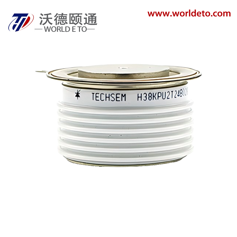
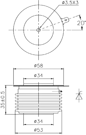
Outline |
KT33dT |