İstisnai istilik sabitliyi və istiliyin daşınması
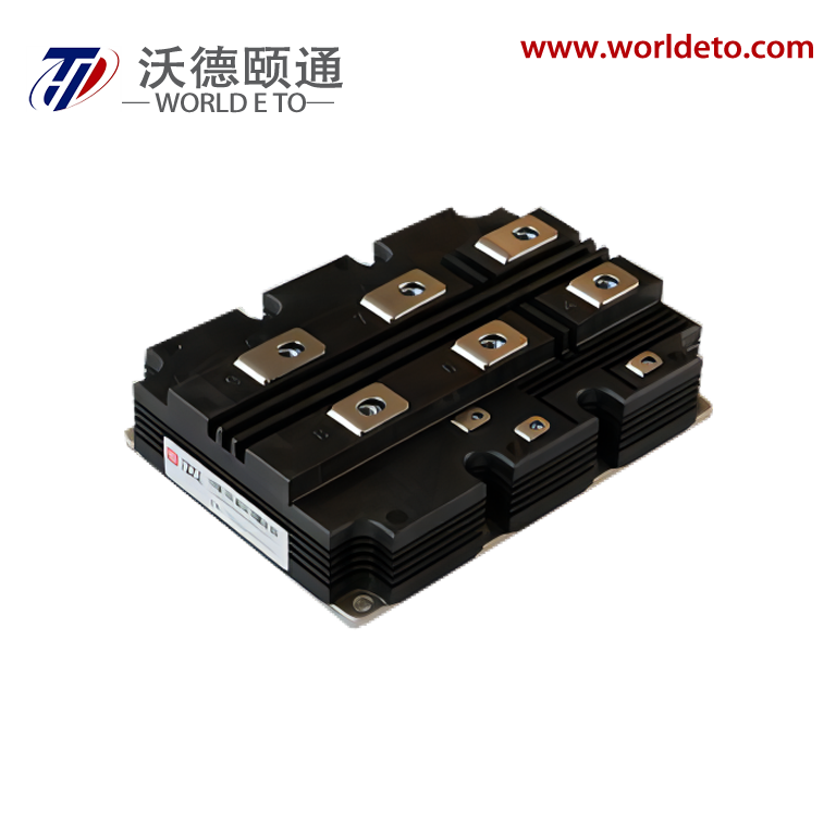
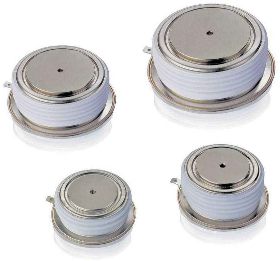
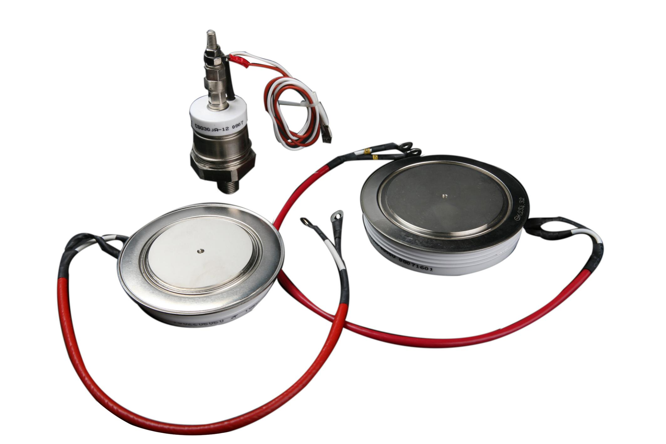
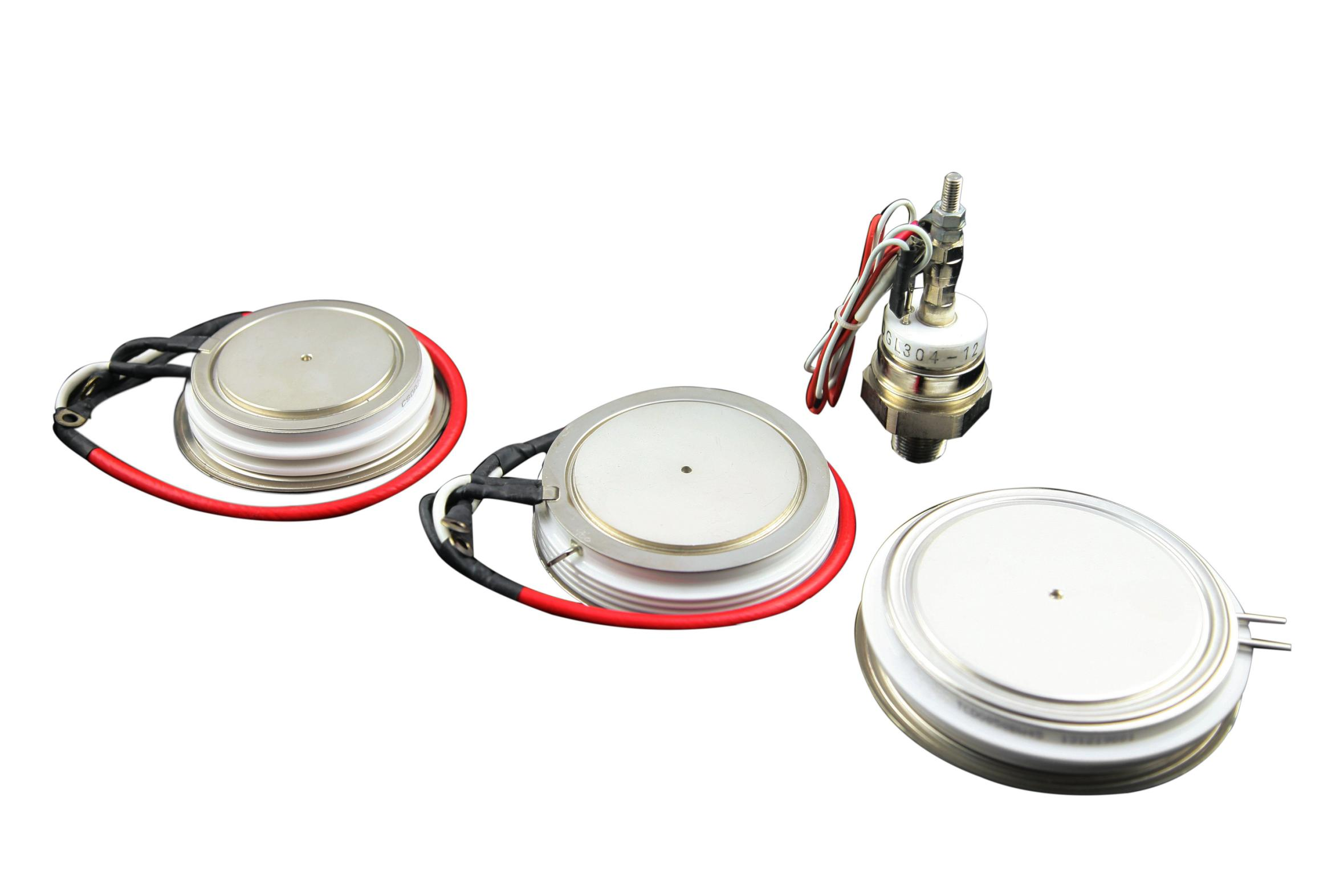
Diod yarımkeçirici plastinlərinin istisnai istilik sabitliyi və istiliyi daşıma qabiliyyəti, temperatur idarə edilməsinin sistem performansı və ömrü üçün həddindən artıq vacib olduğu tələbkar tətbiqlərdə əsas üstünlüklər təmin edir. Yarımkeçirici materialın kristal quruluşu, aktiv keçid nöqtəsindən istiliyi səmərəli şəkildə uzaqlaşdıraraq, isti nöqtələrin yaranmasını və istilikdən qaynaqlanan qeyri-sabitlik (thermal runaway) vəziyyətlərini qarşısını alan yüksək istilikkeçiricilik xüsusiyyətlərinə malikdir. Bu üstün istilik daşıma qabiliyyəti, diod yarımkeçirici plastinlərinin etibarlılığı və ya performansını zədələmədən daha yüksək cərəyan sıxlığı ilə işləməsinə imkan verir. İstilik sabitliyi xüsusiyyətləri, açıq havada işləyən tətbiqlərdə sıfırın altındakı temperaturlardan qapalı elektronik sistemlərdə yüksək temperaturlara qədər geniş temperatur aralığında elektrik xüsusiyyətlərinin sabitliyini təmin edir. İnkişaf etmiş paketləmə texnologiyaları, diod yarımkeçirici plastinlərinin daxili istilik xüsusiyyətlərini xarici istilik yayıcılarına və ya soyutma sistemlərinə effektiv istilik ötürmə yolları təmin edərək tamamlayır. Düzgün dizayn edilmiş diod yarımkeçirici plastinlərinin aşağı istilik müqaviməti, mühərrik sürücüləri, qaynaq avadanlıqları və enerji çevirmə sistemləri kimi yüksək güclü tətbiqlərdə effektiv istilik idarə edilməsini mümkün edir. Diod yarımkeçirici plastinləri üçün temperatur əmsalları spesifikasiyaları, temperatur dəyişiklikləri ilə bağlı performans dəyişikliklərini minimuma endirmək üçün diqqətlə nəzarət olunur; bu da sistem davranışının iş rejimləri boyu proqnozlaşdırıla biləcəyini təmin edir. Diod yarımkeçirici plastinlərinin istilik siklusuna davamlılığı onları dəfələrlə isidilmə və soyudulma sikluslarına tab gətirə bilməyə imkan verir və beləliklə, dəyişən güclü tələblərə malik tətbiqlər üçün ideal hala gətirir. İstilik interfeys materialları və montaj üsulları, yarımkeçirici keçid nöqtəsində istilik gərginliyini minimuma endirmək və istilik ötürmə effektivliyini maksimuma çatdırmaq üçün optimallaşdırılmışdır. Yüksək temperaturda etibarlı işləmə qabiliyyəti, mürəkkəb soyutma sistemlərinə olan ehtiyaçı azaldır, nəticədə sistem dizaynı sadələşir və ümumi xərclər azalır. Genişləndirilmiş temperatur aralığı spesifikasiyaları, diod yarımkeçirici plastinlərinin konvensiyonal komponentlərin uğursuzluğa uğradığı ekstremal mühitlərdə işləməsinə imkan verir ki, bu da onların tətbiq sahələrini və bazar potensialını artırır.