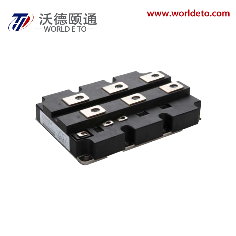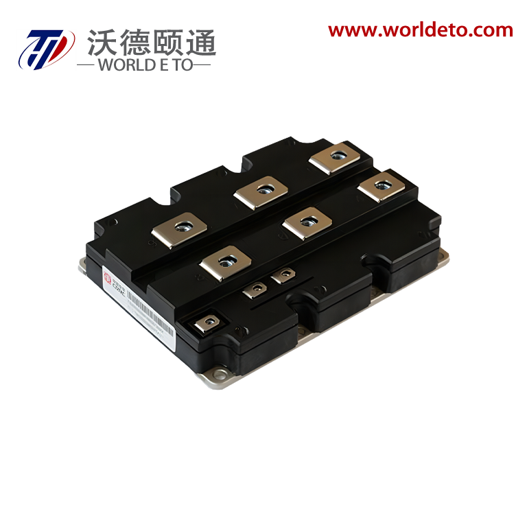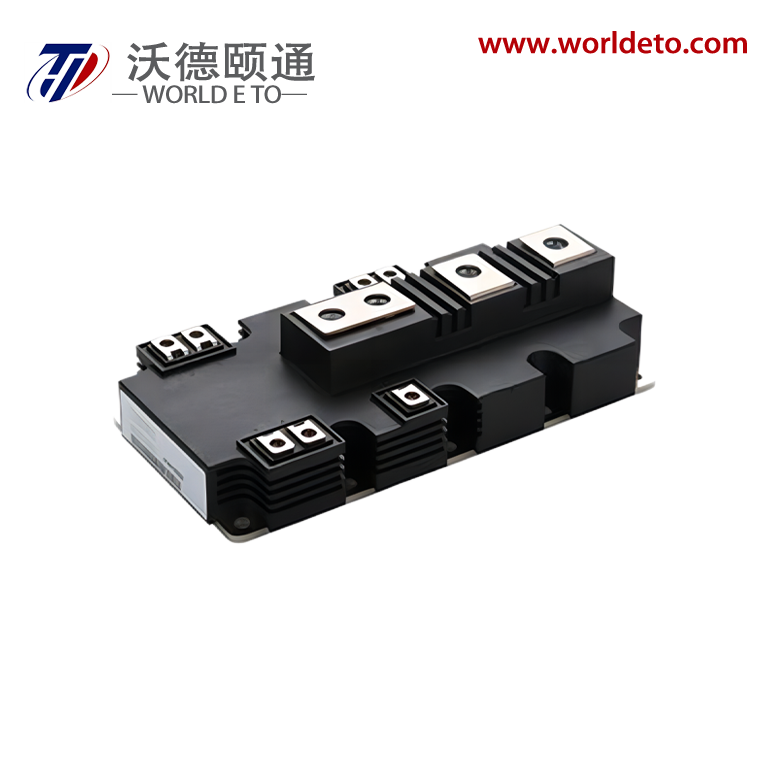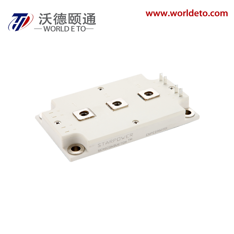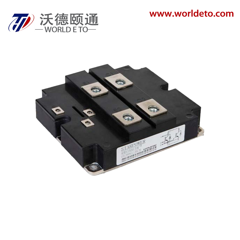
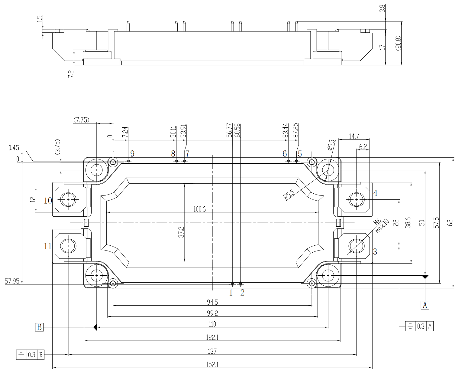
IGBT Module,1200V 450A
Features
Typical Applications
Absolute Maximum Ratings TC=25oC unless otherwise noted
IGBT
Symbol |
Description |
Value |
Unit |
VCES |
Collector-Emitter Voltage |
1200 |
V |
VGES |
Gate-Emitter Voltage |
±20 |
V |
IC |
Collector Current @ TC=25oC @ TC= 100oC |
680 450 |
A |
ICM |
Pulsed Collector Current tp=1ms |
900 |
A |
PD |
Maximum Power Dissipation @ Tj=175oC |
2173 |
W |
Diode
Symbol |
Description |
Value |
Unit |
VRRM |
Repetitive Peak Reverse Voltage |
1200 |
V |
IF |
Diode Continuous Forward Current |
450 |
A |
IFM |
Diode Maximum Forward Current tp=1ms |
900 |
A |
Module
Symbol |
Description |
Value |
Unit |
Tjmax |
Maximum Junction Temperature |
175 |
oC |
Tjop |
Operating Junction Temperature |
-40 to +150 |
oC |
TSTG |
Storage Temperature Range |
-40 to +125 |
oC |
VISO |
Isolation Voltage RMS,f=50Hz,t=1min |
2500 |
V |
IGBT Characteristics TC=25oC unless otherwise noted
Symbol |
Parameter |
Test Conditions |
Min. |
Typ. |
Max. |
Unit |
|
VCE(sat) |
Collector to Emitter Saturation Voltage |
IC=450A,VGE=15V, Tj=25oC |
|
1.70 |
2.15 |
V |
IC=450A,VGE=15V, Tj=125oC |
|
1.95 |
|
|||
IC=450A,VGE=15V, Tj=150oC |
|
2.00 |
|
|||
VGE(th) |
Gate-Emitter Threshold Voltage |
IC= 11.3mA,VCE=VGE, Tj=25oC |
5.2 |
5.8 |
6.4 |
V |
ICES |
Collector Cut-Off Current |
VCE=VCES,VGE=0V, Tj=25oC |
|
|
1.0 |
mA |
IGES |
Gate-Emitter Leakage Current |
VGE=VGES,VCE=0V, Tj=25oC |
|
|
400 |
nA |
RGint |
Internal Gate Resistance |
|
|
0.7 |
|
Ω |
Cies |
Input Capacitance |
VCE=25V,f=1MHz, VGE=0V |
|
46.6 |
|
nF |
Cres |
Reverse Transfer Capacitance |
|
1.31 |
|
nF |
|
QG |
Gate Charge |
VGE=- 15…+15V |
|
3.50 |
|
μC |
td(on) |
Turn-On Delay Time |
VCC=600V,IC=450A, RG= 1.3Ω, VGE=±15V, Tj=25oC |
|
203 |
|
ns |
tr |
Rise Time |
|
64 |
|
ns |
|
td(off) |
Turn-Off Delay Time |
|
491 |
|
ns |
|
tf |
Fall Time |
|
79 |
|
ns |
|
Eon |
Turn-On Switching Loss |
|
16.1 |
|
mJ |
|
Eoff |
Turn-Off Switching Loss |
|
38.0 |
|
mJ |
|
td(on) |
Turn-On Delay Time |
VCC=600V,IC=450A, RG= 1.3Ω, VGE=±15V, Tj= 125oC |
|
235 |
|
ns |
tr |
Rise Time |
|
75 |
|
ns |
|
td(off) |
Turn-Off Delay Time |
|
581 |
|
ns |
|
tf |
Fall Time |
|
109 |
|
ns |
|
Eon |
Turn-On Switching Loss |
|
27.8 |
|
mJ |
|
Eoff |
Turn-Off Switching Loss |
|
55.5 |
|
mJ |
|
td(on) |
Turn-On Delay Time |
VCC=600V,IC=450A, RG= 1.3Ω, VGE=±15V, Tj= 150oC |
|
235 |
|
ns |
tr |
Rise Time |
|
75 |
|
ns |
|
td(off) |
Turn-Off Delay Time |
|
621 |
|
ns |
|
tf |
Fall Time |
|
119 |
|
ns |
|
Eon |
Turn-On Switching Loss |
|
30.5 |
|
mJ |
|
Eoff |
Turn-Off Switching Loss |
|
61.5 |
|
mJ |
|
|
ISC |
SC Data |
tP≤10μs,VGE=15V, Tj=150oC,VCC=800V, VCEM≤1200V |
|
1800 |
|
A |
Diode Characteristics TC=25oC unless otherwise noted
Symbol |
Parameter |
Test Conditions |
Min. |
Typ. |
Max. |
Unit |
|
VF |
Diode Forward Voltage |
IF=450A,VGE=0V,Tj=25oC |
|
1.85 |
2.30 |
V |
IF=450A,VGE=0V,Tj= 125oC |
|
1.90 |
|
|||
IF=450A,VGE=0V,Tj= 150oC |
|
1.95 |
|
|||
Qr |
Recovered Charge |
VCC=600V,IF=450A, -di/dt=6600A/μs,VGE=- 15V, Tj=25oC |
|
55.2 |
|
μC |
IRM |
Peak Reverse Recovery Current |
|
518 |
|
A |
|
Erec |
Reverse Recovery Energy |
|
26.0 |
|
mJ |
|
Qr |
Recovered Charge |
VCC=600V,IF=450A, -di/dt=6600A/μs,VGE=- 15V, Tj= 125oC |
|
106 |
|
μC |
IRM |
Peak Reverse Recovery Current |
|
633 |
|
A |
|
Erec |
Reverse Recovery Energy |
|
47.5 |
|
mJ |
|
Qr |
Recovered Charge |
VCC=600V,IF=450A, -di/dt=6600A/μs,VGE=- 15V, Tj= 150oC |
|
121 |
|
μC |
IRM |
Peak Reverse Recovery Current |
|
661 |
|
A |
|
Erec |
Reverse Recovery Energy |
|
53.9 |
|
mJ |
NTC Characteristics TC=25oC unless otherwise noted
Symbol |
Parameter |
Test Conditions |
Min. |
Typ. |
Max. |
Unit |
R25 |
Rated Resistance |
|
|
5.0 |
|
kΩ |
ΔR/R |
Deviation of R100 |
TC= 100 oC,R100=493.3Ω |
-5 |
|
5 |
% |
P25 |
Power Dissipation |
|
|
|
20.0 |
mW |
B25/50 |
B-value |
R2=R25exp[B25/50(1/T2- 1/(298.15K))] |
|
3375 |
|
K |
B25/80 |
B-value |
R2=R25exp[B25/80(1/T2- 1/(298.15K))] |
|
3411 |
|
K |
B25/100 |
B-value |
R2=R25exp[B25/100(1/T2- 1/(298.15K))] |
|
3433 |
|
K |
Module Characteristics TC=25oC unless otherwise noted
Symbol |
Parameter |
Min. |
Typ. |
Max. |
Unit |
LCE |
Stray Inductance |
|
20 |
|
nH |
RCC’+EE’ |
Module Lead Resistance, Terminal to Chip |
|
1.10 |
|
mΩ |
RthJC |
Junction-to-Case (per IGBT) Junction-to-Case (per Diode) |
|
|
0.069 0.108 |
K/W |
|
RthCH |
Case-to-Heatsink (per IGBT) Case-to-Heatsink (per Diode) Case-to-Heatsink (per Module) |
|
0.030 0.046 0.009 |
|
K/W |
M |
Terminal Connection Torque, Screw M6 Mounting Torque, Screw M5 |
3.0 3.0 |
|
6.0 6.0 |
N.m |
G |
Weight of Module |
|
350 |
|
g |
Our professional sales team are waiting for your consultation.
You can follow their product list and ask any questions you care about.